ChipApex | Global Electronic Components Supplier
SEARCH
Search Product
Search Post
— IC芯片 | 连接器 | 传感器 | 被动器件 —
Search productSearch post
— IC芯片 | 连接器 | 传感器 | 被动器件 —
Consult the customer manager about the wholesale price.
consultation hotline:86-132-6715-2157
email:[email protected]
Contact the product manager for consultation. One-stop consultation is available.
Do you want a lower wholesale price? Please send us your inquiry and we will reply immediately.
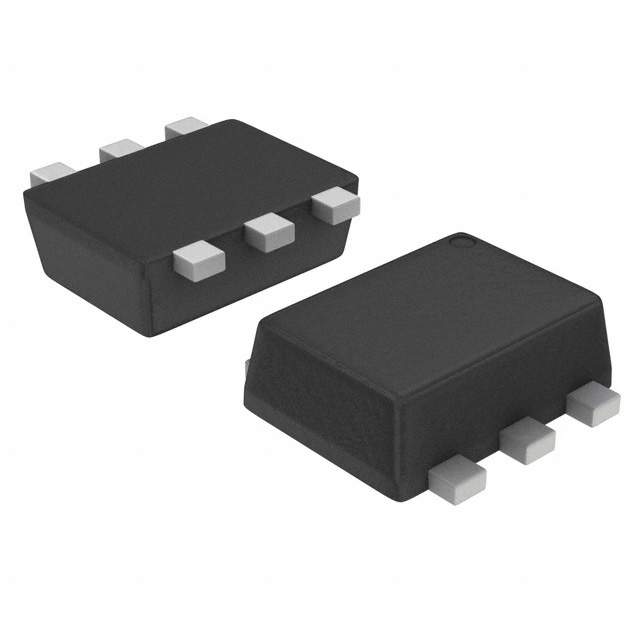
The SSM6P35AFE,LF is a dual P-channel MOSFET manufactured by Toshiba Electronic Devices & Storage Corporation. It utilizes U-MOSVII technology and is housed in an ES6 (SOT-563) package. The device features a drain-source voltage rating of -20 V and a continuous drain current of -250 mA. Typical on-resistance values range from 1.1 Ω at -4.5 V gate drive to 3.2 Ω at -1.2 V. Key dynamic parameters include a typical input capacitance of 21 pF, turn-on delay time of 17 ns, rise time of 42 ns, fall time of 145 ns, and turn-off delay time of 420 ns.
Verify the specific ordering suffix against official Toshiba documentation to confirm packaging format and compliance status. Confirm that the component meets all required environmental standards for the intended deployment environment before finalizing procurement orders.
Select this component when circuit designs require dual P-channel switching with low on-resistance at reduced gate voltages. Ensure the maximum channel temperature does not exceed 150 °C and account for thermal resistance variations based on PCB copper pad area and board thickness during layout.
This part belongs to the SSM6P35AFE series of silicon P-channel MOSFETs. It represents Toshiba's U-MOSVII technology line designed for small-signal applications requiring high efficiency in compact form factors.
SSM6P35AFU,LF
Pin 1 is Source 1, Pin 2 is Gate 1, Pin 3 is Drain 2, Pin 4 is Source 2, Pin 5 is Gate 2, and Pin 6 is Drain 1.
If a reverse bias is applied between the gate and source, the device enters V(BR)DSX mode, which lowers the drain-source breakdown voltage compared to the standard rating.
The typical turn-on delay time is 17 ns, rise time is 42 ns, fall time is 145 ns, and turn-off delay time is 420 ns under specified test conditions.
 SSM6P35AFE,LF
The activity of extra discounts on wholesale prices is in full swing…
Please fill in your contact information and we will send you the latest wholesale price list.