 ChipApex | Global Electronic Components Supplier
SEARCH
Search Product
Search Post
— IC芯片 | 连接器 | 传感器 | 被动器件 —
Search productSearch post
— IC芯片 | 连接器 | 传感器 | 被动器件 —
Consult the customer manager about the wholesale price.
consultation hotline:86-132-6715-2157
email:[email protected]
Contact the product manager for consultation. One-stop consultation is available.
Do you want a lower wholesale price? Please send us your inquiry and we will reply immediately.
The TC6215TG-G is a high-voltage, low-threshold dual MOSFET array featuring independent N-channel and P-channel enhancement-mode transistors in an 8-Lead SOIC package. It integrates back-to-back gate-source Zener diodes for protection. The device guarantees RDS(ON) ratings at 4.0V gate drive, enabling direct interfacing with standard 5.0V CMOS logic. Key electrical parameters include a drain-to-source breakdown voltage of 150V for both channels, a maximum gate threshold voltage of 2.0V, and input capacitance of 120pF (N-channel) or 127pF (P-channel).
Verify the specific ordering suffix to confirm packaging type, such as tape-and-reel or cut tape options. Confirm RoHS compliance status through official manufacturer documentation before finalizing procurement plans. Ensure the component matches the required thermal and electrical specifications for the intended circuit design.
Select this component for applications requiring high voltage handling with low threshold control. The integrated Zener protection simplifies gate drive circuitry. Verify that the operating voltage and current requirements align with the specified absolute maximum ratings and on-state resistance characteristics.
This part belongs to the TC6215 series of dual MOSFET arrays manufactured by Microchip Technology. It utilizes vertical DMOS structure technology to provide bipolar-like power handling with MOSFET input impedance. The 'G' suffix indicates RoHS compliant packaging.
Consult official datasheets for cross-reference data. No public substitute part numbers are confirmed in the provided documentation.
The device includes back-to-back gate-source Zener diodes to clamp the gate voltage and protect against overvoltage conditions.
Yes, the device features guaranteed RDS(ON) ratings down to 4.0V gate drive, allowing direct interfacing with standard 5.0V CMOS logic.
No, the N-channel and P-channel transistors are electrically isolated from each other within the package.
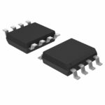 TC6215TG-G
The activity of extra discounts on wholesale prices is in full swing…
Please fill in your contact information and we will send you the latest wholesale price list.





