ChipApex | Global Electronic Components Supplier
SEARCH
Search Product
Search Post
— IC芯片 | 连接器 | 传感器 | 被动器件 —
Search productSearch post
— IC芯片 | 连接器 | 传感器 | 被动器件 —
Consult the customer manager about the wholesale price.
consultation hotline:86-132-6715-2157
email:[email protected]
Contact the product manager for consultation. One-stop consultation is available.
Do you want a lower wholesale price? Please send us your inquiry and we will reply immediately.
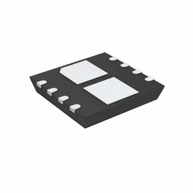
The TC6320K6-G is a high-voltage, low-threshold N-channel and P-channel MOSFET pair manufactured by Microchip Technology. It features an integrated gate-to-source resistor and Zener diode clamp for protection. The device utilizes an advanced vertical DMOS structure to provide high input impedance and fast switching speeds while remaining free from secondary breakdown. It is housed in an 8-lead (4x4) VDFN package with exposed thermal pads.
Verify the specific ordering suffix 'K6' corresponds to the 8-lead DFN package configuration. Confirm that the 'G' suffix indicates lead-free and RoHS compliance as per the manufacturer's product identification system. Ensure the component matches the exact datasheet revision DS20005697A for accurate electrical specifications.
Select this component for applications requiring high-voltage switching with low drive requirements. The complementary N/P-channel design simplifies circuit topology for push-pull configurations. Consider the thermal resistance of the DFN package when designing heat dissipation strategies for continuous operation at elevated temperatures.
This part belongs to the TC6320 family of dual MOSFET arrays. It is functionally similar to the TC6320TG-G but differs in packaging. The K6 suffix specifically denotes the 8-lead (4x4) VDFN package type, which offers a smaller footprint compared to the SOIC variant.
TC6320TG-G
The maximum drain-to-source breakdown voltage (BVDSS) is 200V for the N-channel and -200V for the P-channel.
Yes, it includes integrated gate-to-source resistors and gate-to-source Zener diode clamps.
The typical turn-on delay time (td(ON)) is 10 ns under standard test conditions.
 TC6320K6-G
The activity of extra discounts on wholesale prices is in full swing…
Please fill in your contact information and we will send you the latest wholesale price list.