 ChipApex | Global Electronic Components Supplier
SEARCH
Search Product
Search Post
— IC芯片 | 连接器 | 传感器 | 被动器件 —
Search productSearch post
— IC芯片 | 连接器 | 传感器 | 被动器件 —
Consult the customer manager about the wholesale price.
consultation hotline:86-132-6715-2157
email:[email protected]
Contact the product manager for consultation. One-stop consultation is available.
Do you want a lower wholesale price? Please send us your inquiry and we will reply immediately.
The TC6320TG-G is a high-voltage, low-threshold N-channel and P-channel MOSFET pair in an 8-lead SOIC package. It features integrated gate-to-source resistors and Zener diode clamps for high-voltage pulser applications. The device utilizes an advanced vertical DMOS structure, offering bipolar-like power handling with high input impedance and positive temperature coefficients. Key electrical parameters include a drain-to-source breakdown voltage of 200V, on-state resistance of 7Ω (N-channel) and 8Ω (P-channel), and fast switching speeds with rise/fall times of 15ns.
Verify the specific ordering suffix to confirm the package type and environmental compliance. The 'TG' suffix indicates an 8-lead SOIC package, while 'K6' denotes an 8-lead DFN. Ensure the 'G' suffix is present to confirm lead-free and RoHS-compliant manufacturing standards. Confirm availability through authorized Microchip distributors or direct factory channels.
Select this component when designing circuits requiring high-voltage switching with low drive requirements. The integrated gate protection simplifies driver design by eliminating external clamping components. Consider the thermal resistance of the SOIC package for heat dissipation needs. Verify that the required current ratings align with the specified continuous drain current limits under your operating conditions.
The TC6320 series includes variants such as TC6320K6-G (8-lead DFN) and TC6320TG-G (8-lead SOIC). Both share identical electrical characteristics but differ in physical packaging. The TG variant is suitable for surface mount applications requiring standard SOIC footprint compatibility. This family is designed for high-speed, high-voltage switching applications where reliability and thermal performance are critical.
TC6320K6-G is a pin-compatible alternative in an 8-lead DFN package.
It provides internal clamping to protect the gate oxide from overvoltage stress, which is particularly useful in high-voltage pulser applications.
The device is free from thermal runaway due to the positive temperature coefficient inherent in its MOS structure.
The typical rise time is 15 ns for both N-channel and P-channel devices under specified test conditions.
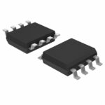 TC6320TG-G
The activity of extra discounts on wholesale prices is in full swing…
Please fill in your contact information and we will send you the latest wholesale price list.





