 ChipApex | Global Electronic Components Supplier
SEARCH
Search Product
Search Post
— IC芯片 | 连接器 | 传感器 | 被动器件 —
Search productSearch post
— IC芯片 | 连接器 | 传感器 | 被动器件 —
Consult the customer manager about the wholesale price.
consultation hotline:86-132-6715-2157
email:[email protected]
Contact the product manager for consultation. One-stop consultation is available.
Do you want a lower wholesale price? Please send us your inquiry and we will reply immediately.
The TC8020K6-G is a six-pair, N- and P-channel enhancement-mode MOSFET array housed in a 56-lead QFN package. It utilizes high-voltage vertical DMOS technology with integrated gate-to-source resistors and Zener diode clamps. The device features a drain-to-source breakdown voltage of 200V for both polarities. Maximum on-state resistance is specified at 9.0Ω for the N-channel and 9.5Ω for the P-channel. Operating temperature ranges from -55°C to +150°C.
Verify the manufacturer origin, as the datasheet identifies Supertex Inc., while distributor listings may attribute it to Microchip Technology due to acquisition history. Confirm the specific suffix 'G' indicates RoHS compliance. Ensure the 56-lead QFN (K6) package matches the design requirements. Check for any specific handling instructions regarding the exposed thermal pad substrate.
Select this component when designing circuits requiring multiple high-voltage switching pairs in a compact footprint. The integrated gate protection simplifies driver circuitry by eliminating external clamping components. Consider the 200V breakdown rating and the specific on-resistance values for power dissipation calculations. Verify that the logic level interface requirements align with the threshold voltage specifications provided in the electrical characteristics.
This component belongs to the TC8020 family of general-purpose MOSFET arrays. Originally developed by Supertex Inc., these devices are characterized by their complementary N- and P-channel configurations. The K6 package variant provides a dense layout suitable for applications where space constraints limit the use of discrete transistors. The device offers thermal stability inherent to MOS structures.
Consult official documentation for verified substitute part numbers. Cross-reference pinouts and electrical parameters carefully if considering alternatives from other manufacturers.
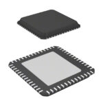 TC8020K6-G
The activity of extra discounts on wholesale prices is in full swing…
Please fill in your contact information and we will send you the latest wholesale price list.





