ChipApex | Global Electronic Components Supplier
SEARCH
Search Product
Search Post
— IC芯片 | 连接器 | 传感器 | 被动器件 —
Search productSearch post
— IC芯片 | 连接器 | 传感器 | 被动器件 —
Consult the customer manager about the wholesale price.
consultation hotline:86-132-6715-2157
email:[email protected]
Contact the product manager for consultation. One-stop consultation is available.
Do you want a lower wholesale price? Please send us your inquiry and we will reply immediately.
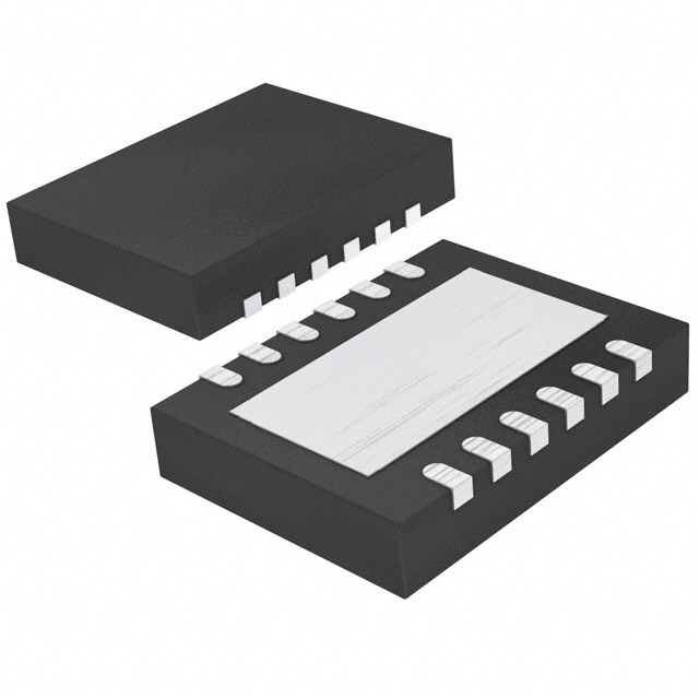
The TC8220K6-G is a high-voltage MOSFET array featuring two pairs of electrically isolated N-channel and P-channel enhancement-mode transistors in a 12-lead DFN package. It utilizes vertical DMOS technology with integrated gate-to-source resistors and Zener diode clamps. The device supports a drain-to-source voltage of 200V, with maximum on-state resistance of 6.5Ω for N-channel and 7Ω for P-channel at 1A. Operating temperature ranges from -55°C to +150°C.
Verify the specific ordering suffix against official Microchip documentation to confirm packaging details. The K6 designation corresponds to the 12-lead DFN package configuration. Ensure environmental compliance requirements match the 'G' suffix specifications. Confirm thermal pad grounding requirements during PCB layout to maintain optimal thermal performance and electrical isolation.
Select this component for designs requiring high-voltage switching with integrated protection features. The built-in gate clamping eliminates external components typically needed for high-voltage gate drive protection. Verify that the 200V breakdown voltage meets system peak voltage requirements. Consider the 12-lead DFN package dimensions for board space constraints and thermal dissipation needs.
This part belongs to the TC8220 family of high-voltage MOSFET arrays manufactured by Microchip Technology. It represents an evolution of vertical DMOS technology designed for robust switching applications. The device integrates multiple functions into a single compact package, reducing component count and board area compared to discrete solutions.
Consult official Microchip documentation for verified substitute part numbers. No cross-references are provided in the source material.
The thermal pad serves as the die attachment substrate and must be grounded externally to ensure proper heat dissipation and electrical operation.
No, the N-channel and P-channel MOSFET pairs within each pair are electrically isolated from each other.
Each gate includes an integrated gate-to-source resistor and a gate-to-source Zener diode clamp for overvoltage protection.
 TC8220K6-G
The activity of extra discounts on wholesale prices is in full swing…
Please fill in your contact information and we will send you the latest wholesale price list.