ChipApex | Global Electronic Components Supplier
SEARCH
Search Product
Search Post
— IC芯片 | 连接器 | 传感器 | 被动器件 —
Search productSearch post
— IC芯片 | 连接器 | 传感器 | 被动器件 —
Consult the customer manager about the wholesale price.
consultation hotline:86-132-6715-2157
email:[email protected]
Contact the product manager for consultation. One-stop consultation is available.
Do you want a lower wholesale price? Please send us your inquiry and we will reply immediately.
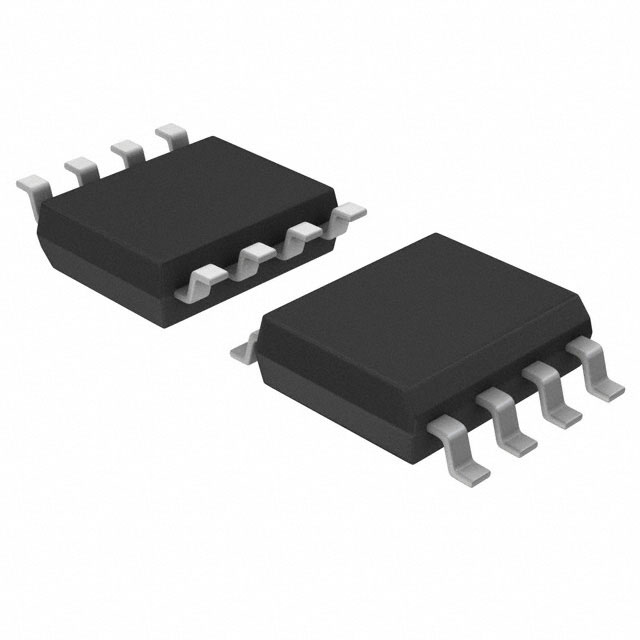
The TPC8207(TE12L) is a dual N-channel silicon MOSFET from Toshiba, utilizing U-MOSIII technology. It features a compact SO-8 package with dimensions of 6.0 mm by 5.0 mm. Key electrical parameters include a drain-source voltage (V_DSS) of 20 V and a continuous DC drain current (I_D) of 6 A at 25°C. The device exhibits a typical drain-source ON-resistance (R_DS(ON)) of 16 mΩ at V_GS = 4.0 V and I_D = 4.8 A. Gate threshold voltage (V_th) ranges from 0.5 V to 1.2 V. Total gate charge (Q_g) is typically 22 nC. Thermal resistance from channel to ambient is 83.3 °C/W for single-device operation on a glass-epoxy board.
Verify the specific ordering suffix TE12L against official Toshiba documentation to confirm reel packaging specifications. Ensure component authenticity through authorized distribution channels. Confirm RoHS compliance status as indicated in the latest datasheet revisions before integration into production designs.
Select this component for applications requiring low R_DS(ON) within a 20 V voltage rating. Evaluate thermal performance based on the specified thermal resistance values for single or dual operation modes. Consider the gate charge requirements for driving circuitry compatibility in high-frequency switching environments.
This part belongs to Toshiba's U-MOSIII series of silicon N-channel MOSFETs. It is designed specifically for portable electronics where space constraints and efficiency are critical. The dual configuration allows for bridge or push-pull applications within a minimal footprint compared to discrete single devices.
Check for direct cross-references in distributor databases. Verify pinout compatibility and electrical parameter margins if substituting with other 20 V dual N-channel MOSFETs in SO-8 packages.
 TPC8207(TE12L)
The activity of extra discounts on wholesale prices is in full swing…
Please fill in your contact information and we will send you the latest wholesale price list.