ChipApex | Global Electronic Components Supplier
SEARCH
Search Product
Search Post
— IC芯片 | 连接器 | 传感器 | 被动器件 —
Search productSearch post
— IC芯片 | 连接器 | 传感器 | 被动器件 —
Consult the customer manager about the wholesale price.
consultation hotline:86-132-6715-2157
email:[email protected]
Contact the product manager for consultation. One-stop consultation is available.
Do you want a lower wholesale price? Please send us your inquiry and we will reply immediately.
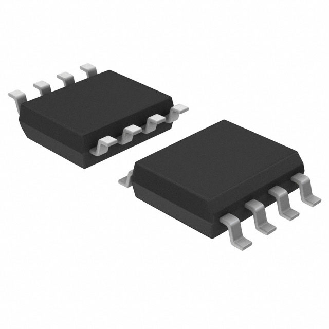
The TPC8213-H is a dual N-channel MOSFET from Toshiba Semiconductor and Storage, utilizing Ultra-High-Speed U-MOSIII technology. It features a PS-8 package with dimensions of 2.9 mm x 2.4 mm x 0.8 mm. Key electrical parameters include a drain-source breakdown voltage (V(BR)DSS) of 60 V, a continuous drain current (ID) of 5 A, and a typical drain-source ON-resistance (RDS(ON)) of 40 mΩ at VGS = 10 V. The device exhibits a total gate charge (Qg) of 11 nC at VDD = 48 V and VGS = 10 V, with a forward transfer admittance (|Yfs|) of 11 S. Maximum power dissipation is 1.5 W for single-device operation on a glass-epoxy board.
Verify the specific ordering suffix TE12LQ against the manufacturer's official documentation to confirm lead-free status and tape-and-reel packaging specifications. Ensure compliance with RoHS directives and check for any regional availability restrictions or end-of-life notices prior to finalizing procurement plans.
Select this component for designs requiring dual N-channel isolation within a minimal footprint. Evaluate thermal resistance values based on the specific PCB copper area and mounting configuration, as power dissipation ratings vary significantly between single and dual operation modes. Confirm that the required gate drive voltage aligns with the specified RDS(ON) performance curves.
This part belongs to Toshiba’s U-MOSIII series of silicon N-channel MOSFETs, engineered for ultra-high-speed switching capabilities. The TPC8213-H specifically targets applications demanding low conduction losses and rapid transient response in small form-factor electronics.
Consult official cross-reference lists for equivalent dual N-channel MOSFETs in PS-8 packages. Verify that substitute parts match the 60 V breakdown voltage, 5 A current rating, and thermal characteristics before implementation.
The maximum channel temperature (Tch) is limited to 150°C.
For single-device operation on board (a), PD is 1.5 W. For single-device value at dual operation on board (a), PD is 1.1 W.
The typical gate switch charge is 2.9 nC under conditions of VDD ≈ 48 V, VGS = 10 V, and ID = 5 A.
 TPC8213-H(TE12LQ,M
The activity of extra discounts on wholesale prices is in full swing…
Please fill in your contact information and we will send you the latest wholesale price list.