ChipApex | Global Electronic Components Supplier
SEARCH
Search Product
Search Post
— IC芯片 | 连接器 | 传感器 | 被动器件 —
Search productSearch post
— IC芯片 | 连接器 | 传感器 | 被动器件 —
Consult the customer manager about the wholesale price.
consultation hotline:86-132-6715-2157
email:[email protected]
Contact the product manager for consultation. One-stop consultation is available.
Do you want a lower wholesale price? Please send us your inquiry and we will reply immediately.
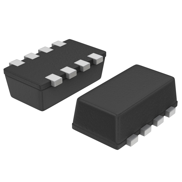
The TPCF8402 is a dual-channel silicon MOSFET featuring one N-channel and one P-channel enhancement-mode device. It utilizes Toshiba's U-MOS IV / U-MOS III technology within a VS8-8 surface-mount package. The N-channel unit provides a drain-source breakdown voltage of 30 V, continuous drain current of 4.0 A, and typical on-resistance of 38 mΩ at VGS = 10 V. The P-channel unit offers a breakdown voltage of -30 V, continuous drain current of -3.2 A, and typical on-resistance of 60 mΩ at VGS = -10 V. Maximum gate-source voltage ratings are ±20 V for both channels.
Verify the specific ordering suffix against official Toshiba Semiconductor documentation to confirm exact packaging and reel specifications. Confirm component availability status as distribution data may indicate end-of-life or discontinuation phases. Ensure compliance with RoHS directives if required by the target application environment. Validate that the VS8-8 package dimensions match the intended PCB footprint layout constraints.
Select this component when a compact solution requires matched N-channel and P-channel switching characteristics. The low on-resistance values support high-efficiency designs in portable devices. Verify thermal dissipation requirements against the specified channel-to-ambient thermal resistance values under expected operating conditions. Ensure gate drive voltages remain within the ±20 V maximum rating limits.
This part belongs to the TPCF series of dual MOSFETs manufactured by Toshiba Semiconductor. The series employs U-MOS technology to achieve low on-resistance and high switching speed in small packages. Similar parts in the lineup include variations with different voltage ratings or current capacities, designed for integration into space-constrained electronic systems requiring complementary switching pairs.
Direct substitutes must match the 30V/4A N-channel and 30V/3.2A P-channel configuration in a VS8-8 package. Verify pinout compatibility and thermal resistance characteristics before substitution. Consult Toshiba's official cross-reference guides for validated alternatives with identical electrical parameters.
The typical RDS(ON) for the N-channel is 38 mΩ when measured at VGS = 10 V and ID = 2.0 A.
The maximum gate-source voltage (V_GSS) rating is ±20 V for both the N-channel and P-channel units.
Yes, the datasheet specifies single-pulse avalanche energy ratings: 2.6 mJ for the N-channel and 0.67 mJ for the P-channel.
 TPCF8402(TE85L,F,M
The activity of extra discounts on wholesale prices is in full swing…
Please fill in your contact information and we will send you the latest wholesale price list.