ChipApex | Global Electronic Components Supplier
SEARCH
Search Product
Search Post
— IC芯片 | 连接器 | 传感器 | 被动器件 —
Search productSearch post
— IC芯片 | 连接器 | 传感器 | 被动器件 —
Consult the customer manager about the wholesale price.
consultation hotline:86-132-6715-2157
email:[email protected]
Contact the product manager for consultation. One-stop consultation is available.
Do you want a lower wholesale price? Please send us your inquiry and we will reply immediately.
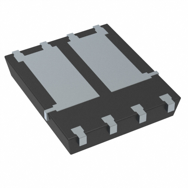
The TSM300NB06DCR RLG is a dual N-Channel Power MOSFET manufactured by Taiwan Semiconductor Corporation. It features a PDFN56 Dual package and operates with a drain-source voltage (VDS) of 60 V. The device supports a continuous drain current of 25 A at case temperature and 6 A at ambient temperature, with a maximum on-state resistance (RDS(on)) of 30 mΩ at VGS = 10 V. Key electrical parameters include a total gate charge (Qg) of 17 nC, a forward transconductance of 24 S, and an input capacitance of 1079 pF. Thermal performance specifies a junction-to-case thermal resistance of 3.1 °C/W.
Verify the specific ordering code TSM300NB06DCR RLG against official Taiwan Semiconductor documentation to confirm package type and packing quantity. Ensure compliance with RoHS standards and halogen-free requirements per IEC 61249-2-21 before procurement. Cross-reference datasheet version A1908 for accurate technical specifications.
Select this component for applications requiring a dual N-Channel MOSFET with a 60 V rating and low conduction losses. Consider the 30 mΩ maximum RDS(on) and 17 nC gate charge for efficiency in DC-DC converters or synchronous rectification. Verify that the operating junction temperature range of -55°C to +150°C meets the environmental requirements of the target system.
This part belongs to the TSM300 series of dual N-Channel Power MOSFETs from Taiwan Semiconductor. It utilizes the PDFN56 Dual surface-mount package, designed for high thermal efficiency and compact footprint. The device is specifically engineered for automotive and industrial applications where reliability under unclamped inductive switching conditions is critical.
Publicly confirmed substitute part numbers are not available in the provided source material. Consult the manufacturer's official documentation for potential cross-references or alternative devices within the same product family.
The maximum continuous drain current is 25 A when measured at a case temperature of 25°C, and 6 A when measured at an ambient temperature of 25°C.
Yes, the device has been tested for 100% UIS capability, with a single pulse avalanche current limit of 12 A and energy limit of 22 mJ.
The maximum junction-to-case thermal resistance (RθJC) is 3.1 °C/W.
 TSM300NB06DCR RLG
The activity of extra discounts on wholesale prices is in full swing…
Please fill in your contact information and we will send you the latest wholesale price list.