ChipApex | Global Electronic Components Supplier
SEARCH
Search Product
Search Post
— IC芯片 | 连接器 | 传感器 | 被动器件 —
Search productSearch post
— IC芯片 | 连接器 | 传感器 | 被动器件 —
Consult the customer manager about the wholesale price.
consultation hotline:86-132-6715-2157
email:[email protected]
Contact the product manager for consultation. One-stop consultation is available.
Do you want a lower wholesale price? Please send us your inquiry and we will reply immediately.
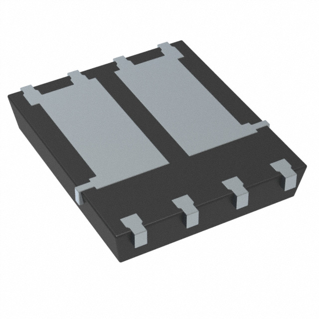
The TSM6502CR is a dual N- and P-channel power MOSFET in a PDFN56 Dual package, rated for 60V drain-source voltage. The N-channel exhibits a maximum RDS(on) of 34mΩ at VGS=10V and 40mΩ at VGS=4.5V, with a continuous drain current of 24A. The P-channel features a maximum RDS(on) of 68mΩ at VGS=-10V and 110mΩ at VGS=-4.5V, supporting a continuous drain current of -18A. Total gate charge is 10.3nC for the N-channel and 9.5nC for the P-channel. Thermal resistance from junction to case is 3.1°C/W, with an operating junction temperature range of -55°C to +150°C.
Verify the specific ordering suffix 'RLG' against the manufacturer's official documentation to confirm reel packaging specifications and quantity. Ensure compliance with RoHS directive 2011/65/EU and WEEE 2002/96/EC standards as stated in the datasheet. Confirm halogen-free status per IEC 61249-2-21 if required by your assembly process.
Select this component for applications requiring complementary N- and P-channel switching in a space-constrained design. The device supports logic-level operation with RDS(on) specified at VGS=4.5V. Verify that the thermal management strategy accounts for the 61°C/W junction-to-ambient resistance when operating without a dedicated heatsink.
This part belongs to Taiwan Semiconductor's lineup of dual MOSFETs designed for efficient power management. It integrates both enhancement-mode N-channel and P-channel transistors into one unit, simplifying bill of materials and board layout for half-bridge or synchronous rectifier topologies.
Publicly confirmed substitute part numbers are not available in the provided source material.
 TSM6502CR RLG
The activity of extra discounts on wholesale prices is in full swing…
Please fill in your contact information and we will send you the latest wholesale price list.