ChipApex | Global Electronic Components Supplier
SEARCH
Search Product
Search Post
— IC芯片 | 连接器 | 传感器 | 被动器件 —
Search productSearch post
— IC芯片 | 连接器 | 传感器 | 被动器件 —
Consult the customer manager about the wholesale price.
consultation hotline:86-132-6715-2157
email:[email protected]
Contact the product manager for consultation. One-stop consultation is available.
Do you want a lower wholesale price? Please send us your inquiry and we will reply immediately.
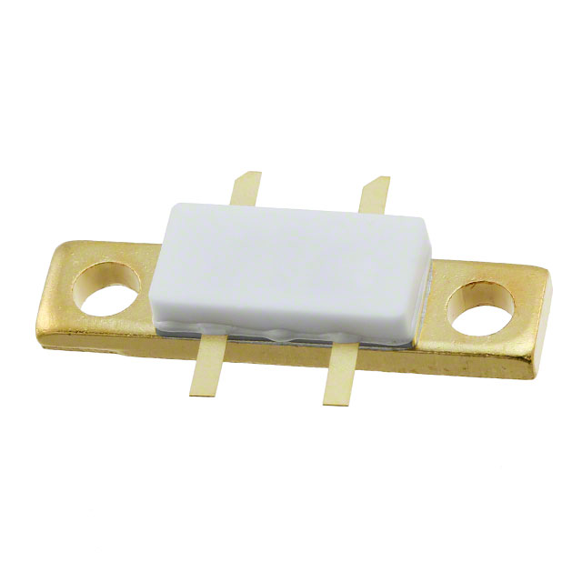
The UF2840G is an N-channel enhancement mode RF power MOSFET transistor manufactured by MACOM Technology Solutions. It operates within a frequency range of 100 MHz to 500 MHz and utilizes a DMOS structure. The device is rated for a drain-source voltage of 65 V and provides a saturated output power of 40 W at a test frequency of 500 MHz with a drain voltage of 28 V. Key electrical characteristics include a typical power gain of 10 dB, a drain efficiency of 50%, and a forward transconductance of 0.5 S. The component supports broadband operation with lower capacitances and exhibits high load mismatch tolerance.
Verify the specific revision status of the datasheet, as it may be marked as Advanced or Preliminary, indicating that performance data is based on target specifications, simulations, or engineering tests rather than guaranteed production volumes. Confirm RoHS compliance status and ensure the ordering suffix matches the required package configuration. Cross-reference impedance values with your specific operating frequency within the 100-500 MHz range.
Select this component when designing circuits requiring 40 W output power across a wide bandwidth from 100 MHz to 500 MHz. Ensure the design accommodates a 28 V drain supply and manages thermal dissipation effectively given the 116 W power rating. Verify that the input and output impedances provided in the datasheet align with your matching network requirements for optimal gain and efficiency at your target frequency.
This part belongs to the MACOM RF Power MOSFET portfolio, specifically engineered for high-performance applications in the VHF/UHF spectrum. It serves as a solid-state replacement for traditional vacuum tubes or other semiconductor technologies in demanding RF environments. The device is characterized for use in systems where reliability, linearity, and broad frequency coverage are critical operational parameters.
No public confirmed substitute part numbers are available in the source documentation.
The device exhibits a load mismatch tolerance of up to 30:1 VSWR under standard test conditions of 28 V drain voltage, 500 mA quiescent current, and 40 W output power at 500 MHz.
The gate threshold voltage (VGS(TH)) ranges from a minimum of 2.0 V to a maximum of 6.0 V, measured with a drain-source voltage of 10.0 V and a drain current of 100.0 mA.
At a drain-source voltage of 28.0 V and a frequency of 1.0 MHz, the typical input capacitance (CISS) is 45 pF, output capacitance (COSS) is 30 pF, and reverse capacitance (CRSS) is 8 pF.
 UF2840G
The activity of extra discounts on wholesale prices is in full swing…
Please fill in your contact information and we will send you the latest wholesale price list.