ChipApex | Global Electronic Components Supplier
SEARCH
Search Product
Search Post
— IC芯片 | 连接器 | 传感器 | 被动器件 —
Search productSearch post
— IC芯片 | 连接器 | 传感器 | 被动器件 —
Consult the customer manager about the wholesale price.
consultation hotline:86-132-6715-2157
email:[email protected]
Contact the product manager for consultation. One-stop consultation is available.
Do you want a lower wholesale price? Please send us your inquiry and we will reply immediately.
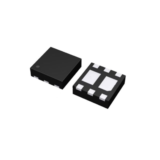
The UT6K3TCR1 is a dual N-channel power MOSFET manufactured by ROHM Semiconductor, housed in a DFN-2020-8D surface-mount package. It features a drain-source voltage (Vds) of 30 V and a continuous drain current (Id) of 5.5 A. The device exhibits a typical on-resistance (Rds(on)) of 42 mΩ at Vgs = 2.5 V. Gate-source voltage limits are ±12 V, with a threshold voltage (Vgs(th)) of 1.5 V. Total gate charge (Qg) is 4 nC. Power dissipation is rated at 2 W, and the maximum operating temperature reaches +150°C. Switching characteristics include a turn-on delay of 7.2 ns, turn-off delay of 13 ns, rise time of 5.8 ns, and fall time of 5.1 ns.
Verify the specific suffix '1' against the official ROHM datasheet to confirm pinout or electrical parameter variations compared to the standard UT6K3TCR variant. Ensure the component meets RoHS compliance requirements for the target assembly process. Confirm that the DFN-2020-8D land pattern matches the manufacturer's recommended layout guidelines to ensure thermal and mechanical reliability during soldering.
Select this component when a dual N-channel MOSFET is required for 30 V applications with high current handling capabilities up to 5.5 A. The low gate charge and fast switching speeds make it suitable for high-frequency DC-DC converters. Verify that the system drive voltage aligns with the specified Vgs range and that the thermal management strategy supports the 2 W power dissipation rating within the desired operating temperature range.
This part belongs to the UT6K series of dual N-channel MOSFETs from ROHM, designed for space-constrained consumer electronics. It serves as an alternative to older packages like SOT-363, offering higher current density in a smaller area. The series is targeted at mobile phones and portable devices requiring efficient power management solutions.
The US6K1 is listed as a similar specification part but uses a different SOT-363T package and has lower current ratings. Direct replacement requires verifying package compatibility and ensuring the lower Id and Rds(on) specifications meet the circuit requirements.
 UT6K3TCR1
The activity of extra discounts on wholesale prices is in full swing…
Please fill in your contact information and we will send you the latest wholesale price list.