 ChipApex | Global Electronic Components Supplier
SEARCH
Search Product
Search Post
— IC芯片 | 连接器 | 传感器 | 被动器件 —
Search productSearch post
— IC芯片 | 连接器 | 传感器 | 被动器件 —
Consult the customer manager about the wholesale price.
consultation hotline:86-132-6715-2157
email:[email protected]
Contact the product manager for consultation. One-stop consultation is available.
Do you want a lower wholesale price? Please send us your inquiry and we will reply immediately.
The ZXMHC3A01N8TC is a complementary enhancement mode MOSFET H-Bridge from Diodes Incorporated, packaged in an SOIC-8. It integrates two N-channel and two P-channel transistors on a single die. The N-channel devices offer a drain-source breakdown voltage of 30V with a maximum continuous drain current of 2.7A at VGS=10V and an on-resistance of 125mΩ. The P-channel counterparts provide a -30V breakdown voltage with a continuous current of -2.1A and an on-resistance of 210mΩ. Both channels operate within a junction temperature range of -55°C to +150°C.
Verify the specific ordering suffix TC against official Diodes Incorporated documentation to confirm reel size and tape width specifications. Ensure the component meets RoHS compliance standards required by your manufacturing process. Cross-reference the manufacturer part number with authorized distributor catalogs to validate authenticity and traceability before finalizing procurement orders.
Select this component when a compact solution for H-Bridge topologies is required. The integrated complementary pair simplifies layout compared to discrete components. Verify that the application's gate drive voltage aligns with the specified thresholds for optimal RDS(on) performance. Consider thermal derating factors based on the PCB copper area and ambient operating conditions.
This device belongs to the ZXMHC3A01 series of complementary MOSFETs manufactured by Diodes Incorporated. It is designed as a direct replacement for other SO-8 packaged H-Bridge solutions requiring similar voltage and current ratings. The series focuses on providing efficient power switching in a minimal footprint for portable and industrial electronics.
Check datasheets for alternative SO-8 complementary MOSFETs with matching 30V ratings and comparable on-resistance values. Ensure pinout compatibility and thermal resistance characteristics align with existing board designs. Verify that substitute components meet the same switching speed and gate charge requirements for the target application.
The maximum continuous drain current for the N-channel device is 2.7A at VGS=10V and TA=25°C.
The total gate charge (Qg) for the P-channel transistor is 5.2nC at VDS=-15V, VGS=-10V, and ID=-1.4A.
The operating junction and storage temperature range is -55°C to +150°C.
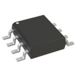 ZXMHC3A01N8TC
The activity of extra discounts on wholesale prices is in full swing…
Please fill in your contact information and we will send you the latest wholesale price list.





