 ChipApex | Global Electronic Components Supplier
SEARCH
Search Product
Search Post
— IC芯片 | 连接器 | 传感器 | 被动器件 —
Search productSearch post
— IC芯片 | 连接器 | 传感器 | 被动器件 —
Consult the customer manager about the wholesale price.
consultation hotline:86-132-6715-2157
email:[email protected]
Contact the product manager for consultation. One-stop consultation is available.
Do you want a lower wholesale price? Please send us your inquiry and we will reply immediately.
The ZXMN3A04DN8TA is a dual N-channel enhancement mode MOSFET from Diodes Incorporated, utilizing TRENCH technology. It features a Drain-Source Voltage (V_DSS) of 30 V and a maximum continuous drain current (I_D) of 8.5 A at 25°C. The device exhibits a low static Drain-Source On-State Resistance (R_DS(on)) of 0.02 Ω at V_GS=10V and 0.03 Ω at V_GS=4.5V. Gate-Source Threshold Voltage (V_GS(th)) is 1.0 V. Thermal resistance (Junction-to-Ambient) ranges from 58 to 100 °C/W depending on PCB copper coverage. Operating temperature spans -55 to +150 °C.
Verify the specific ordering suffix against the manufacturer's official documentation to confirm packaging details. The 'TA' suffix indicates a reel tape width of 7 inches with 12 mm pitch containing 500 units per reel. Confirm that the component meets RoHS compliance standards required for your assembly process before finalizing procurement orders.
Select this component when a compact dual N-channel solution is required for low-voltage power management. Ensure the application operates within the 30 V drain-source voltage limit and accounts for thermal derating factors based on the specific PCB copper area available. Verify that the gate drive voltage supports the specified R_DS(on) performance levels.
This part belongs to the ZXMN3A series of dual N-channel enhancement mode MOSFETs manufactured by Diodes Incorporated under the Zetex brand. The series utilizes TRENCH technology to achieve low on-resistance and fast switching speeds suitable for high-efficiency applications. The device is housed in an SOIC-8 surface mount package.
Consult the manufacturer's datasheet for officially confirmed substitute part numbers. When evaluating alternatives, verify compatibility regarding pinout configuration, voltage ratings, and thermal characteristics to ensure functional equivalence without speculative cross-compatibility claims.
The typical turn-on delay time (t_d(on)) is 5.2 ns, measured at V_DD = 15V, I_D = 1A, R_G = 6.0 Ω, and V_GS = 10V.
No, the switching characteristics are independent of operating junction temperature according to the device specifications.
The typical reverse recovery charge (Q_rr) is 11 nC, measured at T_J = 25°C, I_F = 2.3A, and di/dt = 100A/µs.
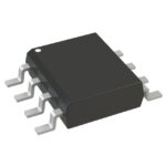 ZXMN3A04DN8TA
The activity of extra discounts on wholesale prices is in full swing…
Please fill in your contact information and we will send you the latest wholesale price list.





