 ChipApex | Global Electronic Components Supplier

SEARCH
Search Product
Search Post
— IC芯片 | 连接器 | 传感器 | 被动器件 —
Search productSearch post
— IC芯片 | 连接器 | 传感器 | 被动器件 —
The trend of science and technology is changing rapidly.
An RF attenuator reduces signal power by a specified amount within an operating frequency range. It helps set signal levels, protect downstream stages and reduce the effects of impedance mismatch. Selection requires more than a dB value: impedance, frequency response, power handling, linearity and control behavior all affect the result.
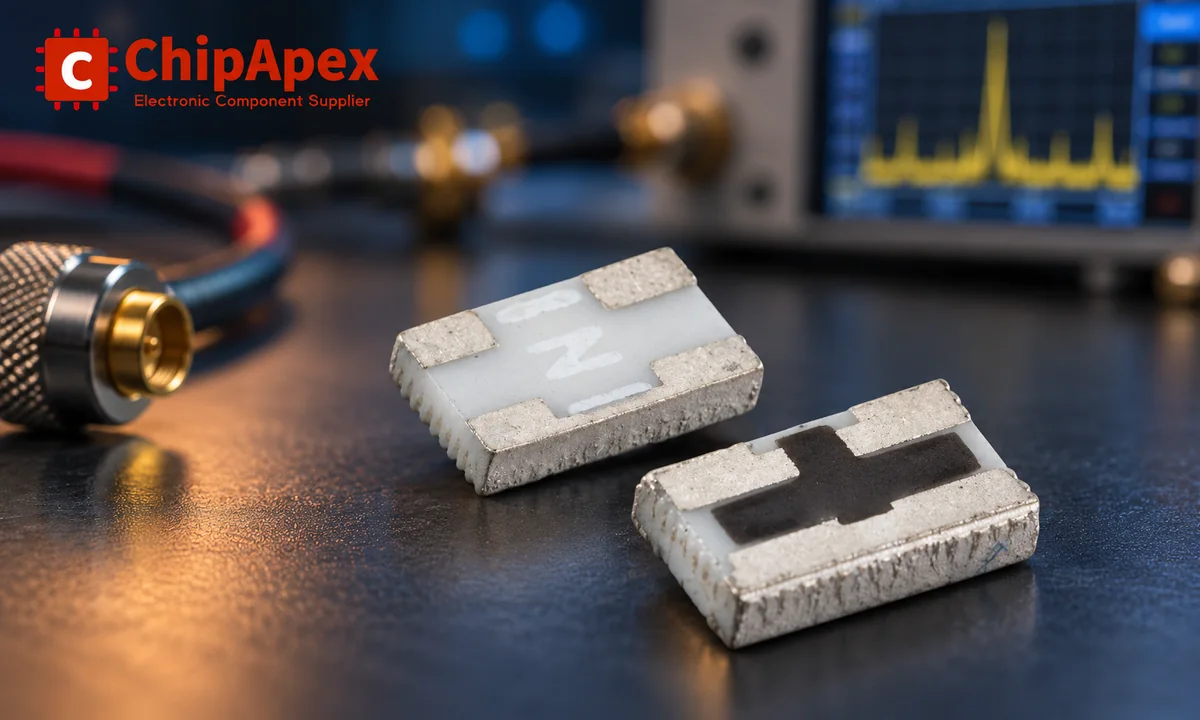
A signal can exceed a receiver's linear range before it reaches a destructive level. An attenuator can bring that signal into a useful measurement or operating range. Fixed pads also help reduce the influence of reflections between imperfectly matched stages.
The loss is intentional. It has a cost in available signal power and, depending on placement, receiver sensitivity. A larger attenuation value is therefore not a general improvement. Choose the amount required by the signal budget.
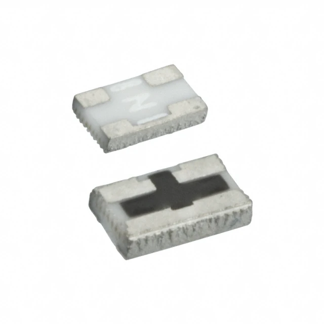
ChipApex's attenuator category includes component options for sourcing. The relevant datasheet establishes whether a device is a fixed chip attenuator, a controlled IC or another format. Package appearance alone cannot establish its electrical behavior.
Optical attenuators and audio power attenuators use different operating conditions and selection criteria from RF components.
For positive attenuation A expressed in decibels:
A = 10 × log10(Pin / Pout)
Pout = Pin × 10^(−A / 10)
When the input and output impedances are equal and voltages use consistent definitions, A = 20 × log10(Vin / Vout). That equal-impedance condition matters; voltage ratio alone does not establish a power ratio between different impedances.
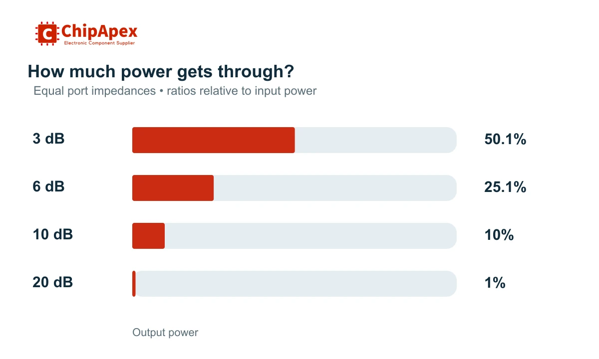
| Attenuation | Output power as a fraction of input | Output voltage ratio at equal impedance |
|---|---|---|
| 3 dB | About 0.501 | About 0.708 |
| 6 dB | About 0.251 | About 0.501 |
| 10 dB | 0.100 | About 0.316 |
| 20 dB | 0.010 | 0.100 |
dB expresses a ratio. dBm expresses an absolute power relative to 1 mW. A +20 dBm input through an ideal 10 dB attenuator becomes +10 dBm, assuming matched ports and the stated attenuation. Connector and cable losses must also be included in a real setup.
| Type | Typical purpose | Main selection question |
|---|---|---|
| Fixed attenuator | Permanent level setting or a known pad in a test path | Is one loss value sufficient across the required band and temperature? |
| Mechanical variable or step attenuator | Manual adjustment on a bench | Are repeatability, connector life and power capability adequate? |
| Voltage-variable attenuator | Continuous level control | Does its control law and distortion suit the control loop? |
| Digital step attenuator | Repeatable programmable gain settings | Are step size, range, switching behavior and interface compatible? |
Fixed resistive attenuators commonly use T or pi networks. Their resistor values establish the intended loss and port match. A simple voltage divider is not automatically a matched RF attenuator.
Controlled designs can use semiconductor switching or variable resistance. Some employ an rf pin diode, while digital designs may switch several attenuation sections. A custom switched-pad arrangement also needs rf switches with suitable loss, isolation and power behavior.
The manufacturer's RF attenuator technical overview explains these configurations and their specification terms. More control capability brings additional questions about supply sequencing, default state and software initialization.
Specify the entire operating band, including harmonics or out-of-band signals that the attenuator must tolerate. Attenuation flatness describes how the loss changes with frequency. A part rated to a high maximum frequency may still have too much variation for a precision amplitude measurement.
Match the specified system impedance. A 50 Ω part in a 75 Ω path can introduce mismatch; an ordinary pad is not a universal impedance transformer. Return loss or VSWR describes the port match under defined conditions. Higher positive return loss and a VSWR closer to 1:1 generally indicate a better match.
For digital parts, check match and attenuation error in every relevant state. The minimum-loss state is not necessarily a lossless through connection. Some datasheets specify attenuation relative to that state, so the absolute path loss includes its insertion loss. Confirm the convention before calculating the receiver level.
For a coaxial assembly, connector type, gender and frequency capability must also fit the test system. For a chip or IC, the PCB layout, grounding and reference plane influence the result. A nominally correct part cannot compensate for an unsuitable RF footprint.
Power handling covers what the device can tolerate under specified conditions. Linearity covers how accurately it preserves the signal before compression or distortion becomes excessive. An absolute maximum input limit, a recommended operating limit and a 1 dB compression point answer different questions.
For a matched passive attenuator, the approximate dissipated power is:
Pdissipated = Pin × (1 − 10^(−A / 10))
A 10 dB pad receiving 1 W delivers about 0.1 W and dissipates about 0.9 W. High attenuation does not make a low-power component suitable for a high-power source. In a cascade, the first pad usually receives the highest power, so equal nominal loss values do not imply equal thermal stress.
Check continuous-wave and peak or pulsed ratings separately, including pulse width, duty cycle and temperature derating. Controlled attenuators may have different limits while switching and while remaining in one state. The maximum loss setting may not be the only limiting state.
For modulated signals, peak envelope power can exceed average power. Compression and intermodulation can spoil measurements even when the component survives. Include the worst-case source level and uncertainty when setting the allowed operating range.
A passive attenuator before a low-noise amplifier reduces both the wanted signal and the signal reaching later nonlinear stages. This can help with a strong interferer, but it also worsens sensitivity. For a matched passive network at the standard reference temperature, its noise figure in dB equals its insertion loss in dB.
Placement after gain generally has a smaller effect on the overall receiver noise figure, although its precise effect depends on the preceding gain and noise contribution. Compare an attenuator before and after rf amplifiers as a system tradeoff rather than assuming the two positions are interchangeable.
A matched pad can also reduce reflections returning through a signal path. Reflected signals traverse it twice, which helps explain why modest loss can improve the effective match seen upstream. The manufacturer's LNA output matching note discusses this application and the placement issue. A pad does not repair every arbitrary load mismatch.
For a digital step attenuator, record the available range, step size and worst-case attenuation error. Resolution is the smallest selectable increment; accuracy describes how close the actual loss is to its specified value. A fine step size does not guarantee fine absolute accuracy.
Read switching time and amplitude settling time separately. Transitions between digital states may produce brief glitches, and some applications also care about phase change. Verify the power-up state, logic levels, control interface and behavior during supply loss.
On a test bench, measure or calibrate the full path, including cables and adapters, across frequency. Include attenuator tolerance in the uncertainty budget. The manufacturer's fixed-attenuator selection guidance starts with the required loss, impedance and maximum input power; those remain the essential first checks.
It approximately halves the power. With equal port impedances, the voltage becomes about 0.708 of the input. About 6 dB attenuation halves voltage under that same condition. State whether a specification concerns power or voltage, and keep the impedance assumption visible when converting between them.
A broadband attenuator reduces level across its specified band. A filter deliberately changes transmission with frequency to pass some frequencies and reject others. Real attenuators still have frequency-dependent loss and a finite operating range. Check their flatness specification when a uniform amplitude reduction is required.
In a suitably matched linear path, their losses in dB add. Two nominal 10 dB pads give approximately 20 dB before accounting for tolerances and mismatch. Check each device's received power separately. Cascading does not allow the first device to exceed its own input or thermal limits.
Usually the minimum state still has insertion loss. Some devices define programmed attenuation relative to that baseline, while other specifications describe absolute loss. Read the datasheet convention and frequency conditions. Include the baseline loss when estimating the signal level delivered to the next stage.
Use the maximum possible source level, the analyzer's operating and damage limits, and a suitable margin for uncertainty. Select attenuation and input power capability together, then check frequency range and connectors. Calibrate or account for the pad and cable loss so the displayed measurement can be referred back to the source.
For ChipApex sourcing, provide the part number or required attenuation, impedance, frequency band, average and peak input power, package and quantity. For controlled parts, include step size, interface and supply requirements.

Learn how NAND flash works, its types (SLC, MLC, TLC), applications in SSDs & embedded systems, and how to source authentic, traceable ICs from trusted suppliers.
View details
Stop guessing which Op-Amp to use. We break down GBWP, Slew Rate, and Offset Voltage with real engineering insights. Find the right parts like NE5532DR & LM358DR at ChipApex.
View details
Choose an AC to DC converter by input range, output demand, isolation, efficiency and thermal derating. Compare architectures and check installation needs.
View details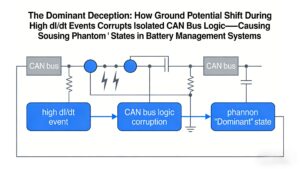
Ground potential shift during high dI/dt regen braking causes isolated CAN receivers to output false dominant states, locking EV BMS networks. Discover robust solutions like TJA1044GT/3Z + common-mode filtering validated by ChipApex.
View details
The activity of extra discounts on wholesale prices is in full swing…
Please fill in your contact information and we will send you the latest wholesale price list.

