 ChipApex | Global Electronic Components Supplier

SEARCH
Search Product
Search Post
— IC芯片 | 连接器 | 传感器 | 被动器件 —
Search productSearch post
— IC芯片 | 连接器 | 传感器 | 被动器件 —
The trend of science and technology is changing rapidly.
A JFET is a junction field-effect transistor. Its gate-to-source voltage controls conduction through a semiconductor channel, with the gate junction normally reverse biased in typical analog use. JFETs are commonly considered for high-input-impedance amplifiers, buffers, analog switching and other circuits where their particular noise and bias characteristics are useful.
A JFET is not interchangeable with any other three-terminal transistor. Channel type, bias range, parameter spread, pin assignment and operating region all matter. This guide explains the parameters that determine whether a device fits a circuit.
In a conventional n-channel JFET, making the gate more negative relative to the source expands the depletion region and reduces channel current. At a sufficiently negative gate-to-source voltage, current falls to a small specified level. A p-channel device uses the opposite polarities.
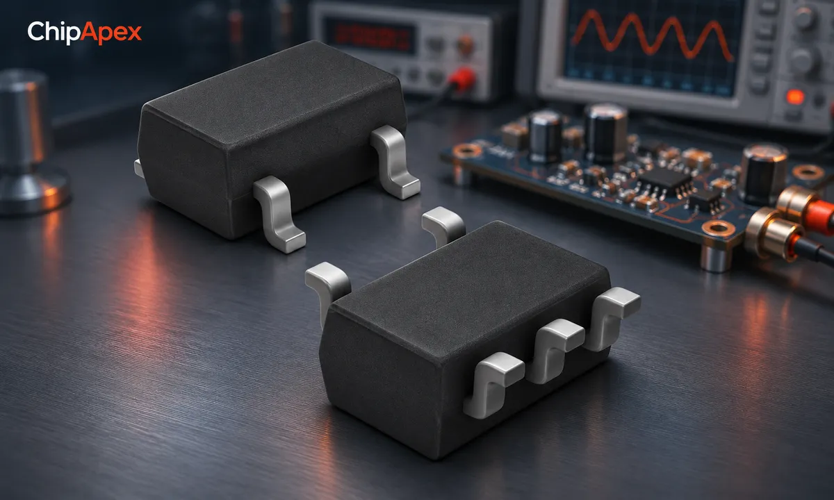
At zero gate-to-source voltage, a conventional depletion-mode JFET conducts when the drain-source operating conditions permit. This differs from the normally-off behavior of a typical enhancement-mode MOSFET. Toshiba's JFET explanation provides background on the junction-controlled channel.
The terms pinch-off and cutoff can cause confusion. Pinch-off in the output characteristic can describe entry into a region where drain current changes relatively little with additional drain voltage. It does not necessarily mean that current is zero. Gate cutoff refers to suppressing conduction with gate bias under stated test conditions.
IDSS describes drain current at zero gate-source voltage under specified drain voltage and temperature. VGS(off) describes the gate-source voltage associated with a small specified drain current. Transconductance describes how much drain current changes for a small gate-source voltage change around an operating point.
| Parameter | Practical relevance |
|---|---|
| IDSS | Starting point for bias-current range |
| VGS(off) | Gate-voltage range needed to reduce conduction |
| Transconductance | Small-signal gain and operating-point behavior |
| Gate leakage | Error with high source impedance |
| Input capacitance | Bandwidth and source-loading effects |
| Noise specifications | Performance at the relevant frequency and bias |
When comparing jfet transistors, read guaranteed ranges rather than relying only on a typical curve. Device-to-device variation can be large enough to move an unadjusted amplifier away from its intended operating point. A circuit designed around one unusually favorable sample may not reproduce across a production batch.
In a simple n-channel self-bias arrangement, a source resistor develops a positive source voltage while the gate is held near a reference potential through a suitable resistance. The resulting negative VGS reduces drain current. The actual operating point follows both the device behavior and the resistor relationship.
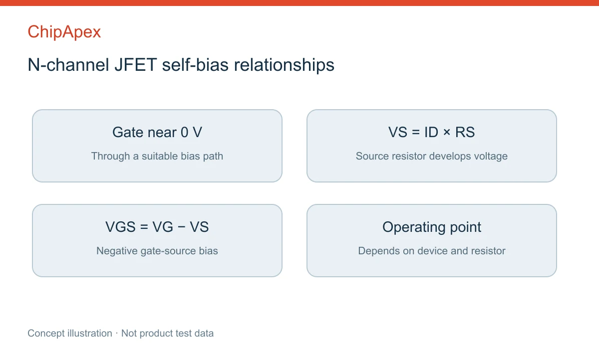
An approximate transfer relationship often used for first estimates is ID = IDSS × (1 − VGS/VGS(off))² within the applicable operating region. It is a model, not a replacement for guaranteed limits or measurement. Near cutoff, in the resistive region or under conditions outside the model's assumptions, it can be inadequate.
Leave enough drain-source voltage for the intended signal swing and operating region. Increasing source resistance changes bias and local feedback; bypassing that resistor changes AC behavior. Evaluate startup and signal overload as well as the quiescent operating point.
A reverse-biased gate draws little current under normal conditions, but leakage is finite and temperature dependent. With a high source resistance, even a small leakage current can create an offset. Board contamination, humidity and protection components may contribute leakage comparable to the transistor itself.
Noise also depends on the source and frequency. A low voltage-noise specification alone does not establish the best device for a high-impedance sensor. Current noise, capacitance, low-frequency behavior and bias conditions can matter. Compare measurements made under relevant conditions rather than assuming all transistors of one type have the same noise advantage.
An instrumentation op amp may be a more direct solution when the system needs a complete differential amplifier with specified gain behavior. A discrete JFET design offers different flexibility and requires its own bias, protection and stability work.
Input capacitance also changes the load seen by a high-impedance source as frequency rises. A device with lower voltage noise may therefore be a poor choice if its capacitance attenuates or distorts the wanted signal. In a hybrid JFET and amplifier design, evaluate the complete input stage, including bias-current sources and loop stability. TI's high-impedance sensor preamplifier brief illustrates these system-level tradeoffs.
JFETs can serve as amplifying devices, switches or voltage-controlled resistive elements under appropriate conditions. Those roles use different parts of the characteristic curves. A device selected for one role is not automatically suitable for another.
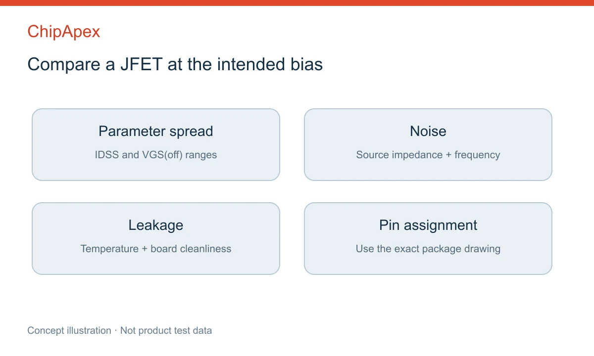
For example, the onsemi J111/J112/J113 datasheet specifies device-dependent cutoff ranges and electrical characteristics for a switching family. Its values should not be generalized to low-noise amplifier JFETs.
Do not assume identical pin order across manufacturers or package variants. Some devices have useful drain-source symmetry in specific applications, but that is not permission to ignore the documented connections and ratings. Also keep the gate junction within its allowed conditions during startup and external signal faults.
A conventional depletion-mode JFET conducts at zero gate-source voltage when suitable drain-source voltage is applied. Reverse gate bias reduces that current. The amount of current depends on the device and operating conditions, so normally on does not mean a fixed current independent of the surrounding circuit.
No. A JFET uses a semiconductor junction at the gate, normally reverse biased in typical operation. A MOSFET uses an insulated gate structure. Their input behavior, protection requirements and operating characteristics differ, even though both are field-effect transistors controlled by gate voltage.
Usually not without reviewing the circuit. The required gate bias, conduction at zero gate voltage, capacitance, noise, pinout and operating region can differ. A replacement that physically fits may establish the wrong current or fail to perform the intended analog function. Check the complete circuit requirements.
IDSS and VGS(off) can vary within the datasheet limits, so the same resistor network can produce different operating currents. A design may need selection, adjustment or feedback to meet a tighter requirement. Use guaranteed parameter ranges to evaluate production variation rather than relying on one measured sample.
No. Noise performance depends on source impedance, frequency, bias current and the specific device. A JFET may be attractive for some high-impedance inputs, but a bipolar transistor or integrated amplifier can be preferable elsewhere. Compare the complete input-referred noise contribution under the intended conditions.
Send ChipApex the existing part number or required channel type, IDSS and cutoff ranges, operating current, noise conditions, package and pinout. For substitutions, include the circuit role and supply voltages. This gives a meaningful basis for comparing candidates without assuming that all JFETs are equivalent.

Choose LED drivers by current, string voltage, dimming and thermal limits. Understand constant-current operation and the checks needed for your load.
View details
A pressure transducer turns pressure into an electrical signal that a controller can read. Inside the device, a sensing element responds to pressure; the electronics then provide a specified voltage, current, or digital output. The output format m...
View details
Learn how rectifiers convert AC to DC, compare half-wave and bridge circuits, and select voltage, current, recovery and thermal ratings for your design.
View details
A positive temperature coefficient (PTC) thermistor is a resistor whose resistance rises as its temperature rises. Depending on its material and curve, that change can be gradual or very steep around a transition temperature. Designers use PTC par...
View details
The activity of extra discounts on wholesale prices is in full swing…
Please fill in your contact information and we will send you the latest wholesale price list.

