 ChipApex | Global Electronic Components Supplier

SEARCH
Search Product
Search Post
— IC芯片 | 连接器 | 传感器 | 被动器件 —
Search productSearch post
— IC芯片 | 连接器 | 传感器 | 被动器件 —
The trend of science and technology is changing rapidly.
A logic circuit inverter, or NOT gate, produces the opposite digital state from its input: a valid low input produces a high output, and a valid high input produces a low output. Choose an inverter IC by supply range, guaranteed input thresholds, output levels, drive conditions and timing. The truth table alone does not establish electrical compatibility.
The term here refers to a digital logic function. A DC-to-AC power inverter is a different class of equipment. Within a digital circuit, an inverter may reverse an enable signal, adapt control polarity or form part of a specified timing arrangement. The surrounding signal conditions determine which device can do that job reliably.
| Input A | Output Y | Condition |
|---|---|---|
| Valid low | High | Supply, loading and input conditions meet the datasheet |
| Valid high | Low | Supply, loading and input conditions meet the datasheet |
| Between guaranteed low and high thresholds | Not defined by the basic truth table | Check the device’s input characteristics and transition requirements |
Logic 0 and logic 1 are ranges of voltages. The boundary between guaranteed low and guaranteed high leaves a region in which an ordinary input’s response is not specified as one stable logic state. A schematic bubble showing inversion does not describe that region.
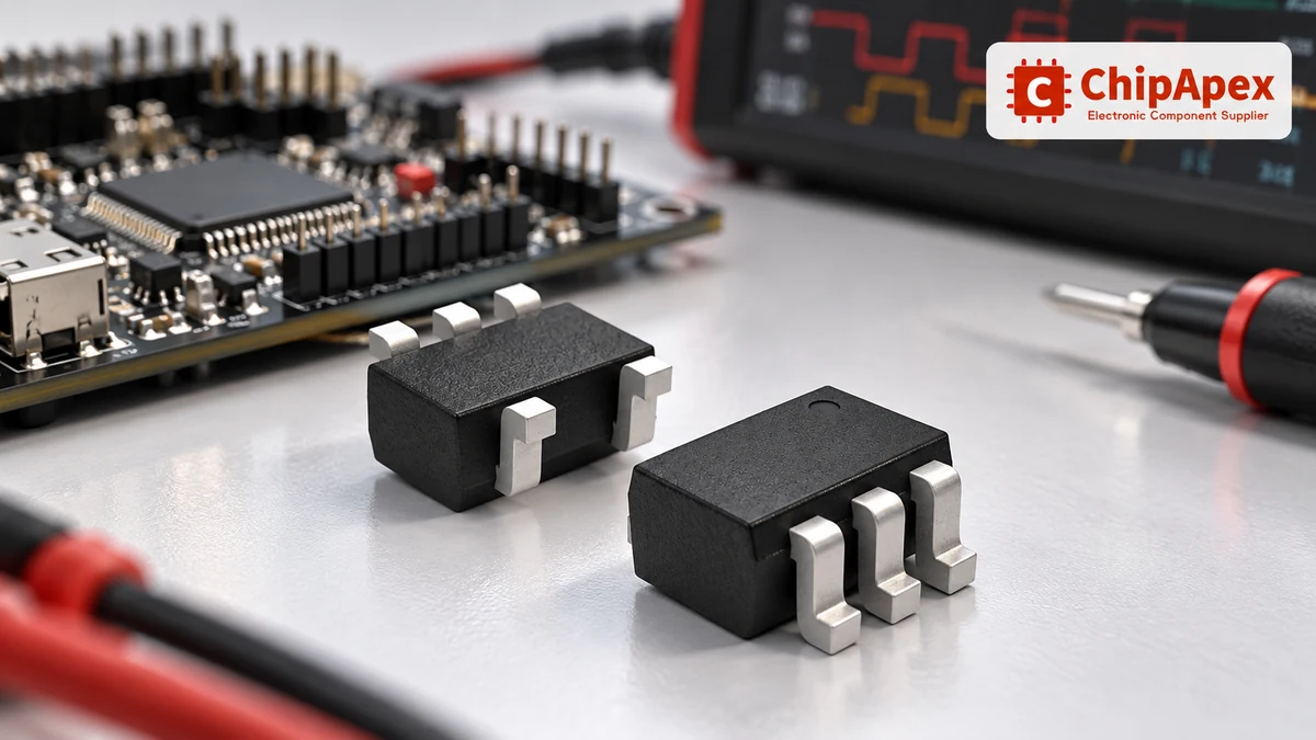
When comparing a logic inverter ic, write down the voltage produced by the previous stage and the voltage required by the next stage. Include tolerance, load and temperature. A part with the correct Boolean function can still fail this interface check.
An ordinary inverter uses its specified input characteristics and requires transitions that meet the datasheet. A Schmitt-trigger inverter has separate thresholds for rising and falling inputs. The difference is hysteresis, which can make an appropriate device more suitable for a slowly changing or noisy signal.
The explanation of Schmitt-trigger CMOS devices illustrates this threshold difference. Hysteresis does not mean that every disturbance is rejected. Noise amplitude, frequency, source impedance and the specified thresholds still matter.
| Input situation | Checks before choosing a device |
|---|---|
| A clean digital output from another IC | Guaranteed voltage levels, transition time, load and timing |
| A slow RC transition | Whether the particular input permits that transition and whether Schmitt behavior is appropriate |
| A mechanical-contact signal | Defined bias, bounce handling and noise protection in addition to threshold behavior |
| An analog signal needing a chosen threshold | Whether a comparator and reference are required instead of relying on a logic input |
If the task is to compare an analog voltage with a defined reference, select a comparator for that purpose. Its input range, output structure and response must be matched to the circuit. An unspecified logic switching point should not become an accidental precision threshold.
For a direct connection, the driver’s guaranteed high output must satisfy the receiver’s required high input under the actual conditions. The corresponding low-output and low-input requirements must also be satisfied. Use worst-case specifications where the datasheet provides them.
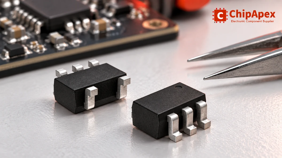
Do not compare a typical output curve at light load with an input limit specified at another supply or temperature and call the interface proven. Output voltage changes with load, while some families’ input thresholds depend strongly on supply voltage. Similar pin names or packages do not remove those differences.
The digital pins on microcontrollers can have different characteristics even within one device. A pin may have a particular threshold type, optional pull resistor, alternate function or supply-domain relationship. Verify the exact pin’s electrical information and reset behavior.
For a sensor interface using an adc converter, review the digital interface separately from the analog input. An inverter in a clock or control path must satisfy the digital timing and voltage requirements. Its presence does not establish that the ADC’s analog range or reference is suitable.
An inverter powered from a lower-voltage rail is not automatically a level translator. Check the input-voltage limits, any stated input tolerance and what happens when its supply is absent. Supply range, input tolerance and output swing are separate specifications.
Likewise, a higher-voltage supply does not guarantee that a lower-voltage signal reaches the required high-input threshold. A family with different threshold conventions may help in a particular case, but that must come from the exact datasheet and operating conditions.
Review power sequencing. One device can remain powered while the next is off, allowing a signal to reach an unpowered input. Check any specified partial-power-down behavior, clamp-current limits or isolation requirements. Do not assume that a normally valid voltage remains acceptable during shutdown or startup.
An inverter may have a push-pull output, an open-drain output or additional control features. A push-pull output actively drives both states within its specified capability. An open-drain output requires an appropriate external pull-up arrangement to establish a high level.
For a push-pull device, compare output-level guarantees at the load current of interest. A maximum current figure elsewhere in the datasheet may not be a recommended operating target. Account for package and total supply-current limits when several gates operate together.
For an open-drain arrangement, the pull-up affects both low-state current and the rising transition. Evaluate receiver capacitance, trace capacitance and leakage. Confirm the output’s allowed voltage and power-off behavior before treating the pull-up rail as a voltage-conversion solution.
A logic inverter should not directly drive a relay coil, motor or other power load unless a particular device and circuit are expressly designed for it. Use the required driver stage and protection. Inversion and load-power handling are different requirements in the circuit specification.
Propagation delay describes how long an output response follows an input event under stated conditions. Review both low-to-high and high-to-low delay where relevant. They can differ, as can their behavior over voltage, temperature and load.
Inserting an inverter also changes polarity and adds a timing element. In a clock path, examine duty-cycle effects, edge quality and the timing relationship seen by receiving devices. A very fast nominal device is not automatically the most suitable choice if its transitions create unnecessary ringing on the board.
When control signals feed flip flops, check setup, hold, clock and asynchronous-control requirements at the receiving device. A change in inverter delay may affect the circuit even if static high and low levels still look correct.
Keep loading explicit. A delay specified with one capacitance does not establish delay with a substantially different cable, connector or collection of inputs. Use the manufacturer’s test conditions and an appropriate signal-integrity review for the actual interconnect.
Floating inputs can respond to interference or remain in an unsuitable intermediate voltage region. Slow transitions through that region can also increase current or create unwanted output activity in devices not intended for them. The application report on slow or floating CMOS inputs explains why input treatment belongs in the design review.
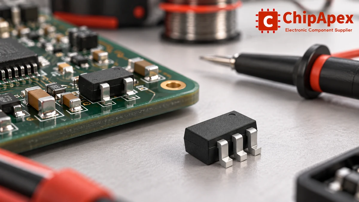
Follow the exact manufacturer’s instructions for unused inputs, bus-hold features and pull resistors. An unused output and an unused input need different treatment. Never tie driven outputs together merely to avoid leaving a pin unconnected.
Place decoupling and return paths according to the device and board requirements. Review supply noise and ground movement alongside input noise; a clean signal referenced to the wrong or moving ground can still violate the receiver’s limits.
For mechanical controls or RC networks, decide where filtering, hysteresis and debounce occur. A Schmitt-trigger input can improve threshold behavior, but it does not by itself guarantee that one mechanical movement produces exactly one application event.
Start with Boolean function, channel count, pinout and package drawing. Then compare supply range, input thresholds, permitted transition behavior, output structure, output levels at load and timing limits. Include temperature, power sequencing and any enable or three-state behavior.
Do not assume that changing a family prefix while retaining the same gate number leaves the circuit unchanged. A faster family may have different input conventions or edge behavior. A smaller package may have different thermal or handling requirements, and a nominally equivalent function may omit a control feature.
Yes, a logic inverter implements the NOT function: a valid high input gives a low output, and a valid low input gives a high output. The part’s electrical specifications determine which voltages represent those states. Channel count, threshold type, output structure and control features can differ between inverter ICs with the same basic truth table.
No. Check the supply range, input tolerance, thresholds, output swing and power-sequencing behavior for the exact device. A signal that is within an absolute maximum limit may still be outside recommended operation or fail a guaranteed input threshold. Use a suitable translator when the required interface cannot be supported by the chosen inverter arrangement.
It can suit an input that changes slowly or contains noise because its rising and falling thresholds differ. The actual threshold limits and permitted input conditions still need to fit the signal. Mechanical contact bounce may create several valid transitions, so an application can need debounce in addition to a Schmitt-trigger input.
Follow the device’s unused-input instructions. Many CMOS inputs need a defined state so they do not respond to noise or remain at an intermediate voltage. Parts with bus-hold or other input features can have different requirements. Confirm how to treat the particular input rather than applying one universal pull-up value to every logic family.
Pin compatibility describes physical connections. It does not prove matching thresholds, output levels, timing, input tolerance or power-off behavior. A replacement may work in one static bench condition yet fail over temperature, loading or startup. Compare the full ordering codes and guaranteed operating conditions against both neighboring stages in the circuit.
An ordinary logic input does not provide a freely selectable precision reference threshold. Its switching behavior follows its specified input characteristics. Use an appropriate comparator and reference when the application needs an analog threshold with defined accuracy or hysteresis. An inverter may still be useful later in the digital control path if its interface requirements are met.
For a ChipApex enquiry, provide the complete original ordering code or the interface requirements, package, channel count and operating conditions. Include quantity and any approved alternatives. Ask for the exact datasheet for the proposed device so engineering can check the receiving and driving circuits together.
Discover why SRAM remains essential in industrial, medical & aerospace systems—thanks to its deterministic performance and long-term reliability. Trusted by engineers worldwide.
View details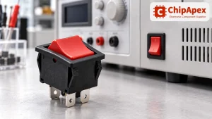
Choose a rocker switch by AC/DC ratings, contact arrangement, illumination, panel fit and sealing. Get practical checks for engineering and component sourcing.
View details
See how a MEMS gyroscope measures angular rate, why its angle estimate drifts, and which range, noise, interface and temperature specs to compare.
View details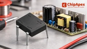
Select a bridge rectifier by reverse voltage, capacitor charging current, startup surge and cooling. Work through a stated DC voltage and ripple example.
View details
The activity of extra discounts on wholesale prices is in full swing…
Please fill in your contact information and we will send you the latest wholesale price list.

