 ChipApex | Global Electronic Components Supplier
SEARCH
Search Product
Search Post
— IC芯片 | 连接器 | 传感器 | 被动器件 —
Search productSearch post
— IC芯片 | 连接器 | 传感器 | 被动器件 —
Consult the customer manager about the wholesale price.
consultation hotline:86-132-6715-2157
email:[email protected]
Contact the product manager for consultation. One-stop consultation is available.
Do you want a lower wholesale price? Please send us your inquiry and we will reply immediately.
The onsemi 2N5952_J35Z is an N-channel RF JFET transistor housed in a TO-92-3 package. It features a Drain-Gate Voltage of 30 V and a Gate-Source Breakdown Voltage of -30 V. The device operates within a junction temperature range of -55°C to +150°C with a total power dissipation of 350 mW at 25°C. Key electrical characteristics include a Zero-Gate Voltage Drain Current (IDSS) ranging from 4.0 mA to 8.0 mA, a Forward Transfer Conductance (gfs) between 2000 µmhos and 6500 µmhos, and a Noise Figure as low as 2.0 dB.
Verify the manufacturer origin carefully, as datasheets indicate Fairchild Semiconductor while distributors list onsemi. Confirm RoHS compliance status through official documentation. Check current production status, as some sources classify this component as obsolete or discontinued. Ensure the specific ordering suffix matches the required packaging configuration before finalizing procurement orders.
Select this component for designs requiring N-channel JFET performance in a TO-92 form factor. Evaluate the IDSS range of 4.0 mA to 8.0 mA against circuit biasing requirements. Consider the thermal resistance values when designing for ambient temperatures exceeding 25°C. Verify that the 350 mW power dissipation limit accommodates the expected operating conditions without excessive derating.
This part belongs to the RF JFET Transistors category. It is historically associated with Fairchild Semiconductor's manufacturing processes, specifically sourced from process 50. The component represents a legacy silicon-based small signal FET solution commonly utilized in vintage or specialized radio frequency equipment designs.
Public confirmed substitute part numbers are not available in the provided documentation. Cross-referencing requires consulting official manufacturer obsolescence notices or equivalent functional replacement guides.
The absolute maximum Gate-Source Voltage (VGS) is rated at -30 V.
The Input Capacitance (Ciss) is typically 6.0 pF at VDS = 15V, VGS = 0, and f = 1.0MHz.
The device has a Total Device Dissipation of 350 mW at 25°C, with a thermal resistance junction-to-ambient of 357 °C/W.
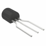 2N5952_J35Z
The activity of extra discounts on wholesale prices is in full swing…
Please fill in your contact information and we will send you the latest wholesale price list.





