 ChipApex | Global Electronic Components Supplier
SEARCH
Search Product
Search Post
— IC芯片 | 连接器 | 传感器 | 被动器件 —
Search productSearch post
— IC芯片 | 连接器 | 传感器 | 被动器件 —
Consult the customer manager about the wholesale price.
consultation hotline:86-132-6715-2157
email:[email protected]
Contact the product manager for consultation. One-stop consultation is available.
Do you want a lower wholesale price? Please send us your inquiry and we will reply immediately.
The onsemi 2N5953_J35Z is an N-Channel RF Amplifier JFET in a TO-92-3 package. It features a Drain-Gate Voltage of 30 V and Gate-Source Voltage of -30 V, with a maximum junction temperature of 150 °C. The device provides a Zero-Gate Voltage Drain Current (IDSS) ranging from 2.5 mA to 5 mA at 15 V. Small signal characteristics include a Forward Transfer Conductance (gfs) between 1000 μ/Ω and 6500 μ/Ω at 100 MHz, Input Capacitance (Ciss) of 6 pF, and Reverse Transfer Capacitance (Crss) of 2 pF at 1.0 MHz.
Verify the component status carefully, as the original manufacturer datasheet indicates this product may be obsolete or discontinued by Fairchild Semiconductor. Confirm current availability and sourcing channels through authorized distributors. Ensure that any replacement components meet the required electrical specifications and thermal characteristics for your specific application needs.
Select this component based on its N-Channel configuration and RF amplifier capabilities. Consider the absolute maximum ratings, specifically the 30 V voltage limits and 150 °C junction temperature. Evaluate the small signal characteristics like input capacitance and forward transfer conductance to ensure compatibility with your circuit's frequency and gain requirements.
The 2N5953 is part of the 2N595x series of N-Channel RF Amplifiers originally manufactured by Fairchild Semiconductor. This series includes variants such as the 2N5950, 2N5951, and 2N5952, which share similar packaging and basic operational principles but may differ in specific electrical parameters. The 2N5953_J35Z designation indicates a specific ordering suffix for this particular variant.
Check for direct substitutes within the 2N595x series, such as the 2N5950_J35Z or 2N5952_J35Z, ensuring their electrical parameters align with your design requirements. Verify if other manufacturers offer equivalent N-Channel JFETs with comparable voltage ratings and small signal characteristics.
The 2N5953 is designed primarily for electronic switching applications, particularly those requiring low on-resistance analog switching.
The absolute maximum ratings include a Drain-Gate Voltage of 30 V and a Gate-Source Voltage of -30 V.
The noise figure is specified as 2 dB at 1.0 kHz with a source resistance of 1.0 mΩ, and 5 dB at 100 MHz with a source resistance of 1.0 kΩ.


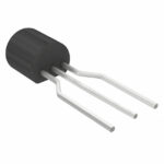 2N5953_J35Z
The activity of extra discounts on wholesale prices is in full swing…
Please fill in your contact information and we will send you the latest wholesale price list.




