 ChipApex | Global Electronic Components Supplier
SEARCH
Search Product
Search Post
— IC芯片 | 连接器 | 传感器 | 被动器件 —
Search productSearch post
— IC芯片 | 连接器 | 传感器 | 被动器件 —
Consult the customer manager about the wholesale price.
consultation hotline:86-132-6715-2157
email:[email protected]
Contact the product manager for consultation. One-stop consultation is available.
Do you want a lower wholesale price? Please send us your inquiry and we will reply immediately.
The Infineon Technologies 2N7002DWH6327XTSA1 is a dual N-channel OptiMOS™ small-signal MOSFET in a PG-SOT363 package. It features a 60 V drain-source breakdown voltage and logic-level operation with a maximum RDS(on) of 3 Ω at VGS=10 V and 4 Ω at VGS=4.5 V. The device supports a continuous drain current of 0.3 A, pulsed current up to 1.2 A, and power dissipation of 0.5 W. It includes avalanche rating capabilities, fast switching characteristics, and an integrated reverse diode.
Verify the specific ordering suffix H6327XTSA1 against official Infineon documentation to confirm tape and reel packaging quantities and marking codes. Ensure compliance with RoHS and halogen-free requirements as specified in the datasheet. Confirm that the component meets AEC-Q101 qualification standards if automotive application is intended.
Select this component when a compact dual N-channel solution is required for logic-level switching. The SOT363 package minimizes board space while providing sufficient thermal management for 0.5 W dissipation. Consider the 3 Ω on-resistance at 10 V gate drive for efficient conduction in low-current paths.
This part belongs to the 2N7002DW series of OptiMOS™ small-signal transistors manufactured by Infineon Technologies. It utilizes silicon technology and is designed for surface-mount assembly. The device integrates two independent N-channel MOSFETs within a single six-lead outline, offering a cost-effective alternative to discrete single-transistor implementations.
Cross-reference with other manufacturers' 2N7002 equivalents such as those from ON Semiconductor or Panjit. Verify pinout compatibility and electrical parameter margins, particularly RDS(on) and VGS(th), before substitution.
Yes, the device is qualified according to AEC-Q101 standards.
The single pulse avalanche energy is rated at 1.3 mJ under conditions of ID=0.3 A and RGS=25 Ω.
No, the component is halogen-free according to IEC61249-2-21.
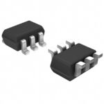 2N7002DWH6327XTSA1
The activity of extra discounts on wholesale prices is in full swing…
Please fill in your contact information and we will send you the latest wholesale price list.





