 ChipApex | Global Electronic Components Supplier

SEARCH
Search Product
Search Post
— IC芯片 | 连接器 | 传感器 | 被动器件 —
Search productSearch post
— IC芯片 | 连接器 | 传感器 | 被动器件 —
Consult the customer manager about the wholesale price.
consultation hotline:86-132-6715-2157
email:[email protected]
Contact the product manager for consultation. One-stop consultation is available.
Do you want a lower wholesale price? Please send us your inquiry and we will reply immediately.
74ALVC16827MTDX is listed in the Buffers, Drivers, Receivers, Transceivers range at ChipApex. The manufacturer field lists onsemi. Its product description is IC BUF NON-INVERT 3.6V 56TSSOP. Review the specifications below when checking this part for your BOM.
The onsemi 74ALVC16827MTDX is a low voltage 20-bit buffer and line driver featuring 3.6V tolerant inputs and outputs. It contains twenty non-inverting buffers with 3-state outputs, designed for memory, address, clock drivers, or bus-oriented transmitter/receiver applications carrying parity. The device operates within a supply voltage range of 1.65V to 3.6V and utilizes advanced CMOS technology for high-speed operation with low power dissipation. Propagation delays are specified at 3.0 ns max for 3.0V to 3.6V VCC, 3.5 ns max for 2.3V to 2.7V VCC, and 6.0 ns max for 1.65V to 1.95V VCC.
Verify the specific ordering code suffix when sourcing components. The datasheet indicates that devices are available on tape and reel; specify by appending the suffix letter “X” to the standard ordering code. Confirm package details match the required 56-lead thin shrink small outline package (TSSOP) specifications before procurement.
Select this component for designs requiring 20-bit buffering with 3.6V I/O tolerance in low voltage environments. Ensure the application supports byte-controlled functionality using independent NOR output enables. Verify that the operating temperature range of -40°C to +85°C meets system requirements and that the 56-TSSOP package fits the PCB layout constraints.
This part belongs to the ALVC logic family, characterized by low voltage operation and high speed. It serves as a buffer and line driver solution for systems needing wide data path expansion. The device is manufactured using advanced CMOS technology to balance performance with power efficiency in portable and battery-operated applications.
Check for pin-compatible alternatives from other manufacturers offering similar 20-bit buffer specifications. Ensure replacement parts maintain the 3.6V I/O tolerance and operate within the same 1.65V to 3.6V supply voltage range. Verify propagation delay characteristics match the original design timing requirements.
The 3-state outputs are controlled by Output Enable (OE_n) inputs. When OE1 and OE2 are LOW, O0–O10 are in the 2-state mode. If either OE1 or OE2 is HIGH, the outputs enter a high impedance state.
Floating or unused control inputs must be held HIGH or LOW to ensure proper device operation and prevent undefined states.
Explore related parts through Logic, Integrated Circuits (ICs), all product categories, ChipApex homepage.
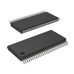 74ALVC16827MTDX
Understand tactile switches, PCB and keyboard differences, four-pin wiring, debounce, force, travel and replacement checks for reliable control inputs.
Read More
Select a common mode choke using noise frequency, current, insulation and signal integrity. Understand impedance curves, layout and filter limitations.
Read More
74ALVC16827MTDX is listed in the Buffers, Drivers, Receivers, Transceivers range at ChipApex. The manufacturer field lists onsemi. Its product description is IC BUF NON-INVERT…
Read More
74ALVC16827MTDX is listed in the Buffers, Drivers, Receivers, Transceivers range at ChipApex. The manufacturer field lists onsemi. Its product description is IC BUF NON-INVERT…
Read More
74ALVC16827MTDX is listed in the Buffers, Drivers, Receivers, Transceivers range at ChipApex. The manufacturer field lists onsemi. Its product description is IC BUF NON-INVERT…
Read More
74ALVC16827MTDX is listed in the Buffers, Drivers, Receivers, Transceivers range at ChipApex. The manufacturer field lists onsemi. Its product description is IC BUF NON-INVERT…
Read More
74ALVC16827MTDX is listed in the Buffers, Drivers, Receivers, Transceivers range at ChipApex. The manufacturer field lists onsemi. Its product description is IC BUF NON-INVERT…
Read More
74ALVC16827MTDX is listed in the Buffers, Drivers, Receivers, Transceivers range at ChipApex. The manufacturer field lists onsemi. Its product description is IC BUF NON-INVERT…
Read More
Compare RC, crystal and MEMS oscillator circuits. Check ppm, jitter, load capacitance, startup margin and output compatibility before choosing a clock source.
Read More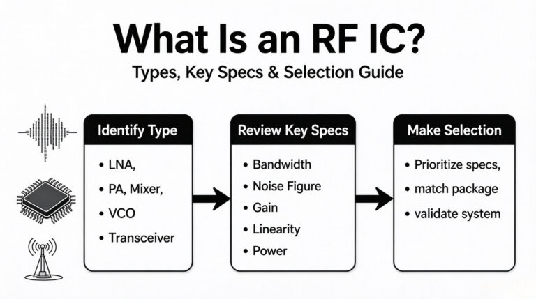
74ALVC16827MTDX is listed in the Buffers, Drivers, Receivers, Transceivers range at ChipApex. The manufacturer field lists onsemi. Its product description is IC BUF NON-INVERT…
Read More
74ALVC16827MTDX is listed in the Buffers, Drivers, Receivers, Transceivers range at ChipApex. The manufacturer field lists onsemi. Its product description is IC BUF NON-INVERT…
Read More
Choose an ADC converter by resolution, sample rate, noise and input design. Review practical tradeoffs and prepare component requirements for ChipApex.
Read More
The activity of extra discounts on wholesale prices is in full swing…
Please fill in your contact information and we will send you the latest wholesale price list.





