 ChipApex | Global Electronic Components Supplier

SEARCH
Search Product
Search Post
— IC芯片 | 连接器 | 传感器 | 被动器件 —
Search productSearch post
— IC芯片 | 连接器 | 传感器 | 被动器件 —
Consult the customer manager about the wholesale price.
consultation hotline:86-132-6715-2157
email:[email protected]
Contact the product manager for consultation. One-stop consultation is available.
Do you want a lower wholesale price? Please send us your inquiry and we will reply immediately.
The AO4818BL_101 is a dual N-channel enhancement mode field effect transistor manufactured by Alpha & Omega Semiconductor Inc. It utilizes advanced trench technology to deliver low on-resistance and gate charge, making it suitable for load switch and PWM applications. The device features a drain-source voltage of 30V and a continuous drain current of 8A at VGS=10V. Key electrical parameters include an RDS(ON) of less than 19mΩ at VGS=10V and less than 26mΩ at VGS=4.5V. It operates within a junction temperature range of -55°C to 150°C and is housed in an 8-SOIC package.
Verify the specific ordering suffix against official manufacturer documentation to confirm exact packaging and marking details. Confirm RoHS compliance status directly from the datasheet before procurement. Ensure the component meets all applicable export control regulations and legal requirements for your intended use case.
Select this component for circuits requiring a dual N-channel MOSFET with a 30V rating. Evaluate thermal performance based on the specific board copper area and ambient conditions, as the junction-to-ambient resistance varies significantly with layout. Consider the low gate charge for high-frequency switching efficiency.
This part belongs to the AO4818 series of dual N-channel MOSFETs from Alpha & Omega Semiconductor. The 'B' variant typically denotes specific electrical or packaging revisions within the product line. The base model shares similar trench technology features but may differ in exact parameter tolerances or testing standards.
Publicly confirmed substitute part numbers are not available in the provided source material. Verify pinout compatibility and absolute maximum ratings if considering alternative manufacturers.
The maximum pulsed drain current (IDM) is 48A, limited by the junction temperature.
Yes, the datasheet specifies that the device undergoes 100% UIS testing.
The typical body diode reverse recovery time (trr) is 6ns, with a maximum of 10ns under specified test conditions.
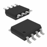 AO4818BL_101

The activity of extra discounts on wholesale prices is in full swing…
Please fill in your contact information and we will send you the latest wholesale price list.





