 ChipApex | Global Electronic Components Supplier

SEARCH
Search Product
Search Post
— IC芯片 | 连接器 | 传感器 | 被动器件 —
Search productSearch post
— IC芯片 | 连接器 | 传感器 | 被动器件 —
Consult the customer manager about the wholesale price.
consultation hotline:86-132-6715-2157
email:[email protected]
Contact the product manager for consultation. One-stop consultation is available.
Do you want a lower wholesale price? Please send us your inquiry and we will reply immediately.
The AO4914 is a dual N-channel MOSFET integrated with a Schottky diode, utilizing advanced trench technology for low on-resistance and gate charge. It features two independent N-channel FETs (Q1 and Q2) each rated for a drain-source voltage of 30V and a continuous drain current of 8A at VGS=10V. The on-resistance is less than 20.5mΩ at VGS=10V and 28mΩ at VGS=4.5V. The co-packaged Schottky diode supports a forward current of 3A with a maximum forward voltage of 0.5V at 1A. The device operates within a junction temperature range of -55°C to 150°C and is housed in an SOIC-8 package.
Verify component authenticity through authorized distributors or direct manufacturer channels. Confirm datasheet revision status matches design requirements. Ensure storage conditions adhere to moisture sensitivity level specifications. Validate thermal management solutions align with specified junction-to-ambient resistance values. Check for any specific handling precautions outlined in the official documentation.
Evaluate thermal dissipation capabilities based on specific board copper area and airflow conditions. Consider gate drive voltage levels to ensure optimal RDS(ON) performance. Assess switching frequency requirements against gate charge specifications. Verify compatibility with system voltage rails and current loads. Review safe operating area curves for transient load conditions.
This component belongs to Alpha & Omega Semiconductor's discrete MOSFET portfolio, specifically designed for high-efficiency power switching applications. The integration of a Schottky diode distinguishes it from standard dual MOSFET packages by offering additional rectification functionality without extra board space.
Publicly confirmed substitute part numbers are not available in the provided source material. Consult official AOS documentation for potential cross-reference recommendations.
Each N-channel MOSFET supports a continuous drain current of 8A when the gate-source voltage is 10V.
The Schottky diode is co-packaged in parallel with the synchronous MOSFET to boost efficiency further by providing a low-loss path for body diode conduction.
Yes, both MOSFETs are 100% UIS tested to ensure reliability under inductive load switching conditions.
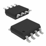 AO4914_101

The activity of extra discounts on wholesale prices is in full swing…
Please fill in your contact information and we will send you the latest wholesale price list.





