 ChipApex | Global Electronic Components Supplier

SEARCH
Search Product
Search Post
— IC芯片 | 连接器 | 传感器 | 被动器件 —
Search productSearch post
— IC芯片 | 连接器 | 传感器 | 被动器件 —
Consult the customer manager about the wholesale price.
consultation hotline:86-132-6715-2157
email:[email protected]
Contact the product manager for consultation. One-stop consultation is available.
Do you want a lower wholesale price? Please send us your inquiry and we will reply immediately.
The AO6601 is a complementary enhancement mode field effect transistor utilizing advanced trench technology to deliver low gate charge and excellent on-resistance. The N-Channel device supports a drain-source voltage of 30V with a continuous drain current of 3.4A at VGS=10V, while the P-Channel counterpart handles -30V and -2.3A respectively. Both channels feature low RDS(ON) values across various gate voltages, enabling efficient power inversion in high-speed applications.
Verify the specific datasheet revision (e.g., Rev 6.1) matches your design requirements. Confirm that the TSOP6 package dimensions align with your PCB footprint. Ensure thermal management strategies account for the junction-to-ambient resistance specified in the absolute maximum ratings table.
Select this component when a compact complementary pair is required for low-voltage switching applications. Evaluate the RDS(ON) specifications against your load current needs at the intended operating gate voltage. Consider the thermal constraints defined by the maximum junction temperature and power dissipation limits.
This part belongs to Alpha & Omega Semiconductor's complementary MOSFET lineup. It is designed as a cost-effective solution for consumer electronics where space and efficiency are critical. The TSOP6 package allows for surface-mount assembly, facilitating automated manufacturing processes.
Check pinout compatibility before substitution. Verify that any alternative device meets or exceeds the 30V breakdown voltage and current handling capabilities. Ensure the replacement package type matches the existing board layout to avoid mechanical integration issues.
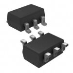 AO6601

The activity of extra discounts on wholesale prices is in full swing…
Please fill in your contact information and we will send you the latest wholesale price list.





