 ChipApex | Global Electronic Components Supplier
SEARCH
Search Product
Search Post
— IC芯片 | 连接器 | 传感器 | 被动器件 —
Search productSearch post
— IC芯片 | 连接器 | 传感器 | 被动器件 —
Consult the customer manager about the wholesale price.
consultation hotline:86-132-6715-2157
email:[email protected]
Contact the product manager for consultation. One-stop consultation is available.
Do you want a lower wholesale price? Please send us your inquiry and we will reply immediately.
The AO8814#A is a dual N-channel enhancement mode MOSFET array manufactured by Alpha & Omega Semiconductor Inc. It features a common-drain configuration housed in an 8-TSSOP surface-mount package. The device supports a drain-source voltage (Vdss) of 20V and a continuous drain current (Id) of 7.5A at 25°C. Key electrical parameters include a maximum on-resistance (Rds(on)) of 16mΩ at Vgs=10V, a gate charge (Qg) of 14nC at Vgs=4.5V, and an input capacitance (Ciss) of 1295pF at Vds=10V. It operates within a junction temperature range of -55°C to 150°C with a maximum power dissipation of 1.5W.
Verify the specific suffix #A against the manufacturer's official documentation to confirm exact pinout compatibility and RoHS compliance status. Confirm that the 8-TSSOP package dimensions match the target PCB footprint. Ensure that the sourcing channel provides valid traceability records for this discontinued or legacy component series.
Select this component when a compact dual N-channel solution is required for low-voltage applications. The 20V rating and 7.5A current capacity suit portable electronics. Compare Rds(on) and Qg values against alternatives to ensure efficiency targets are met. Verify thermal dissipation capabilities within the 1.5W limit for the intended enclosure environment.
This part belongs to the AO881 family of dual MOSFET arrays from Alpha & Omega Semiconductor. It shares architectural similarities with the AO8810 and AO8812 but differs in specific current ratings and package variants. The AO8814 specifically targets high-density power applications requiring two matched N-channel transistors in a single small outline package.
The maximum gate-source voltage (Vgs) is ±20V.
Yes, the component is specified as lead-free and compliant with RoHS standards.
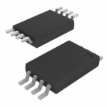 AO8814#A
The activity of extra discounts on wholesale prices is in full swing…
Please fill in your contact information and we will send you the latest wholesale price list.





