 ChipApex | Global Electronic Components Supplier
SEARCH
Search Product
Search Post
— IC芯片 | 连接器 | 传感器 | 被动器件 —
Search productSearch post
— IC芯片 | 连接器 | 传感器 | 被动器件 —
Consult the customer manager about the wholesale price.
consultation hotline:86-132-6715-2157
email:[email protected]
Contact the product manager for consultation. One-stop consultation is available.
Do you want a lower wholesale price? Please send us your inquiry and we will reply immediately.
The AOB410L is a 100V N-Channel Enhancement Mode Field Effect Transistor manufactured by Alpha & Omega Semiconductor Inc. utilizing SDMOS™ trench technology. It features a maximum drain current of 150A and an on-state resistance below 6.5mΩ at VGS=10V. The device operates within a junction temperature range of -55°C to 175°C and is supplied in a TO-263 (D2PAK) surface mount package.
Verify the specific ordering suffix 'L' against official Alpha & Omega Semiconductor documentation to confirm compliance with Green Product specifications. Ensure the selected package variant matches the required thermal management strategy for the intended application environment.
Select this component based on its 100V rating and 150A continuous current capability. Evaluate the thermal resistance parameters relative to the system's heatsinking requirements. Confirm that the gate drive voltage aligns with the specified thresholds for optimal on-resistance performance.
This part belongs to the SDMOS™ family of N-Channel MOSFETs from Alpha & Omega Semiconductor. It shares design similarities with the AOT410L, differing primarily in packaging format. The product line emphasizes high current density and low conduction losses for power electronics.
The AOT410L is electrically identical but utilizes a TO-220 tube package instead of the TO-263 tape and reel format. Verify mechanical footprint compatibility before substitution.
Yes, the datasheet confirms that the device undergoes 100% Unclamped Inductive Switching (UIS) testing.
The maximum junction and storage temperature range is -55°C to 175°C.
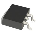 AOB410L
The activity of extra discounts on wholesale prices is in full swing…
Please fill in your contact information and we will send you the latest wholesale price list.





