ChipApex | Global Electronic Components Supplier

SEARCH
Search Product
Search Post
— IC芯片 | 连接器 | 传感器 | 被动器件 —
Search productSearch post
— IC芯片 | 连接器 | 传感器 | 被动器件 —
Consult the customer manager about the wholesale price.
consultation hotline:86-132-6715-2157
email:[email protected]
Contact the product manager for consultation. One-stop consultation is available.
Do you want a lower wholesale price? Please send us your inquiry and we will reply immediately.
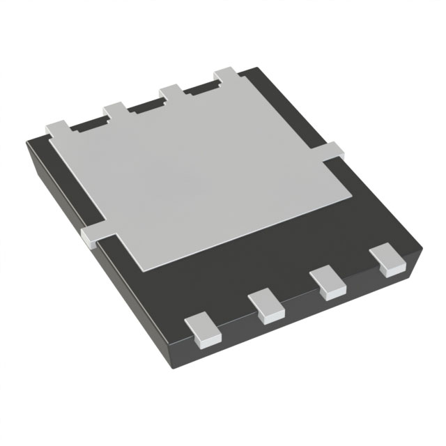
AON6290 is listed in the Single FETs, MOSFETs range at ChipApex. The manufacturer field lists Alpha & Omega Semiconductor Inc.. Its product description is MOSFET N CH 100V 28A DFN5X6. Review the specifications below when checking this part for your BOM.
The AON6290 is a 100V N-Channel MOSFET utilizing trench technology optimized for high-frequency switching. It features an on-resistance of less than 4.6mΩ at VGS=10V and 6.2mΩ at VGS=6V, with a continuous drain current of 85A. The device supports a pulsed drain current of 180A and operates within a junction temperature range of -55°C to 150°C. Packaged in DFN5X6, it includes 100% UIS and Rg testing.
Verify the specific package variant and tape/reel specifications against the manufacturer's latest ordering information before finalizing procurement plans. Ensure that thermal management designs account for the specified junction-to-ambient and junction-to-case thermal resistances under actual operating conditions. Confirm compliance with RoHS3 standards and check for any recent design changes or lifecycle status updates directly from Alpha & Omega Semiconductor documentation.
Select this component when designing circuits requiring a 100V rating with high current handling capabilities up to 85A continuous. The low on-resistance makes it suitable for applications prioritizing efficiency in power conversion stages. Consider the DFN5X6 package constraints for PCB layout and thermal dissipation requirements. Evaluate the gate charge characteristics against driver capabilities to ensure optimal switching speeds in high-frequency environments.
The AON6290 belongs to Alpha & Omega Semiconductor's portfolio of power MOSFETs designed for advanced electronics. It leverages proprietary trench technology to deliver superior performance compared to standard planar devices. This series targets demanding power supply applications where size, weight, and efficiency are critical factors in system design.
No public confirmed substitute part numbers are available in the provided documentation.
The maximum pulsed drain current is 180A.
Yes, the device undergoes 100% Unclamped Inductive Switching (UIS) testing.
The junction and storage temperature range is -55°C to 150°C.
Explore related parts through FETs, MOSFETs, Transistors, Discrete Semiconductor Products, all product categories.
 AON6290

The activity of extra discounts on wholesale prices is in full swing…
Please fill in your contact information and we will send you the latest wholesale price list.