 ChipApex | Global Electronic Components Supplier

SEARCH
Search Product
Search Post
— IC芯片 | 连接器 | 传感器 | 被动器件 —
Search productSearch post
— IC芯片 | 连接器 | 传感器 | 被动器件 —
Consult the customer manager about the wholesale price.
consultation hotline:86-132-6715-2157
email:[email protected]
Contact the product manager for consultation. One-stop consultation is available.
Do you want a lower wholesale price? Please send us your inquiry and we will reply immediately.
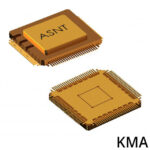
ASNT7123A-KMA is listed in the Analog To Digital Converters (ADC) range at ChipApex. The manufacturer field lists ADSANTEC. Its product description is 20GH 16GS 4-BIT FLASH ADC W/ PLL. Review the specifications below when checking this part for your BOM.
The ASNT7123A-KMA is a 4-bit flash analog-to-digital converter (ADC) featuring a 20 GHz analog input bandwidth and a sampling rate up to 16 GS/s. It operates from a single +3.5 V supply with a power consumption of 4.62 W. The device supports selectable clocking modes, including an external high-speed clock or an internal PLL with a central frequency of 10 GHz driven by an LVDS reference clock. Key features include a broadband operation range of DC-16 GS/s in external clocking mode, on-chip PRBS generation for output data scrambling, and differential CML input/output buffers. The component is housed in a custom 100-pin metal-ceramic package.
Verify the specific ordering suffix KMA corresponds to the 100-pin metal-ceramic CQFP package configuration. Confirm that the required thermal management solutions accommodate the 4.62 W power dissipation and junction temperature limits specified in the datasheet. Ensure compatibility with the single +3.5 V power supply requirement and 2.5V CMOS control logic levels.
Select this component when a 4-bit resolution at sampling rates up to 16 GS/s is sufficient for the application. Consider the internal PLL if a stable LVDS reference clock is available, otherwise utilize the external clocking mode for frequencies up to 16 GHz. Evaluate the need for the integrated PRBS generator and DAC for built-in self-test capabilities. Ensure the PCB design supports the differential CML I/O requirements and proper termination strategies.
The ASNT7123A-KMA belongs to the ADSANTEC high-frequency integrated circuit family, specifically designed for broadband digital and analog signal processing. It complements other multiplexers and demultiplexers in the portfolio by providing high-speed digitization capabilities. The device utilizes advanced fabrication technology to achieve wide bandwidth and low jitter performance in a robust metal-ceramic package suitable for demanding environments.
Publicly confirmed substitute part numbers are not available in the provided documentation. When evaluating alternatives, ensure the replacement matches the 16 GS/s sampling rate, 20 GHz bandwidth, 4-bit resolution, and 100-pin CQFP package dimensions. Verify compatibility with the +3.5 V supply voltage and CML interface standards.
The CMU operates in 'clock multiplication' mode (PLL enabled, reference clock applied to crp/crn) or 'clock division' mode (PLL disabled, external high-speed clock applied to cep/cen).
Threshold voltages are controlled by analog signals vrefcrl and vlsbcrl. vrefcrl shifts the DC levels of all thresholds, while vlsbcrl alters the LSB voltage range and shifts DC levels.
The PRBS generator produces a 32-kbit pseudo-random binary sequence using polynomial x^15+x^14+1. It can be mixed with output data via the scrambler for testing or disabled to pass data unchanged.
Explore related parts through Data Acquisition, Integrated Circuits (ICs), all product categories, ChipApex homepage.
 ASNT7123A-KMA

ASNT7123A-KMA is listed in the Analog To Digital Converters (ADC) range at ChipApex. The manufacturer field lists ADSANTEC. Its product description is 20GH 16GS…
Read More
ASNT7123A-KMA is listed in the Analog To Digital Converters (ADC) range at ChipApex. The manufacturer field lists ADSANTEC. Its product description is 20GH 16GS…
Read More
ASNT7123A-KMA is listed in the Analog To Digital Converters (ADC) range at ChipApex. The manufacturer field lists ADSANTEC. Its product description is 20GH 16GS…
Read More
ASNT7123A-KMA is listed in the Analog To Digital Converters (ADC) range at ChipApex. The manufacturer field lists ADSANTEC. Its product description is 20GH 16GS…
Read More
ASNT7123A-KMA is listed in the Analog To Digital Converters (ADC) range at ChipApex. The manufacturer field lists ADSANTEC. Its product description is 20GH 16GS…
Read More
ASNT7123A-KMA is listed in the Analog To Digital Converters (ADC) range at ChipApex. The manufacturer field lists ADSANTEC. Its product description is 20GH 16GS…
Read More
ASNT7123A-KMA is listed in the Analog To Digital Converters (ADC) range at ChipApex. The manufacturer field lists ADSANTEC. Its product description is 20GH 16GS…
Read More
ASNT7123A-KMA is listed in the Analog To Digital Converters (ADC) range at ChipApex. The manufacturer field lists ADSANTEC. Its product description is 20GH 16GS…
Read More
ASNT7123A-KMA is listed in the Analog To Digital Converters (ADC) range at ChipApex. The manufacturer field lists ADSANTEC. Its product description is 20GH 16GS…
Read More
ASNT7123A-KMA is listed in the Analog To Digital Converters (ADC) range at ChipApex. The manufacturer field lists ADSANTEC. Its product description is 20GH 16GS…
Read More
ASNT7123A-KMA is listed in the Analog To Digital Converters (ADC) range at ChipApex. The manufacturer field lists ADSANTEC. Its product description is 20GH 16GS…
Read More
Learn how rectifiers convert AC to DC, compare half-wave and bridge circuits, and select voltage, current, recovery and thermal ratings for your design.
Read More
The activity of extra discounts on wholesale prices is in full swing…
Please fill in your contact information and we will send you the latest wholesale price list.





