ChipApex | Global Electronic Components Supplier
SEARCH
Search Product
Search Post
— IC芯片 | 连接器 | 传感器 | 被动器件 —
Search productSearch post
— IC芯片 | 连接器 | 传感器 | 被动器件 —
Consult the customer manager about the wholesale price.
consultation hotline:86-132-6715-2157
email:[email protected]
Contact the product manager for consultation. One-stop consultation is available.
Do you want a lower wholesale price? Please send us your inquiry and we will reply immediately.
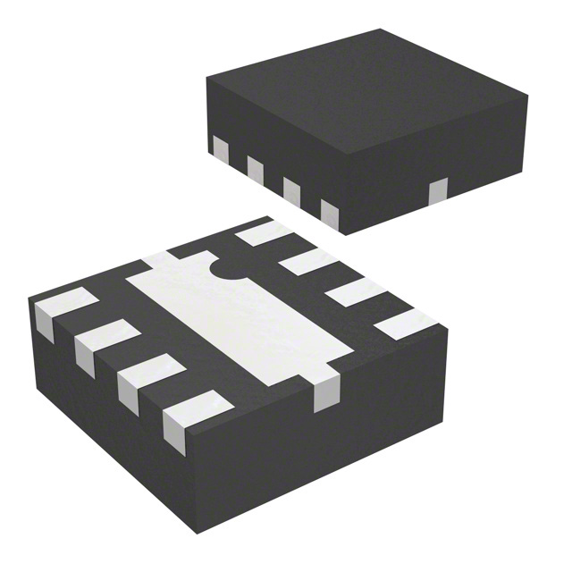
The Broadcom ATF-511P8 is a single-voltage, high linearity enhancement mode pseudomorphic HEMT housed in an 8-lead JEDEC-standard leadless plastic chip carrier (LPCC) package measuring 2.0 x 2.0 x 0.75 mm. Operating from 50 MHz to 6 GHz, it functions as a medium-power amplifier with excellent uniformity. At 2 GHz and 4.5V/200 mA bias, it delivers a typical gain of 14.8 dB, noise figure of 1.4 dB, output IP3 of 41.7 dBm, P1dB of 30 dBm, and PAE of 69%. The device utilizes backside metalization for thermal dissipation and visual solder reflow verification.
Verify the specific ordering suffix against official documentation to confirm packaging configuration. The BLK suffix indicates antistatic bag packaging containing 100 units, whereas TR1 and TR2 variants correspond to tape-and-reel configurations. Ensure compatibility with required supply quantities and handling standards before procurement.
Select this component for designs requiring high linearity and moderate power output within the Sub-6 GHz range. Verify that the PCB layout accommodates the 2x2 mm LPCC footprint and provides adequate thermal vias for the exposed drain pad. Confirm bias circuitry supports the single positive Vgs requirement without negative gate supplies.
This device belongs to the family of enhancement mode pseudomorphic HEMTs designed for RF power amplification. It replaces conventional depletion mode devices by simplifying bias requirements. The ATF-511P8 is manufactured using GaAs pHEMT technology, offering a balance of gain, linearity, and efficiency in a compact surface-mount package.
Public confirmed substitute part numbers are not available in the provided datasheet. Designers should consult manufacturer application notes or cross-reference databases for compatible alternatives if the ATF-511P8 is unavailable.
The operational gate voltage ranges from 0.25 V to 0.8 V when biased at Vds = 4.5V and Ids = 200 mA.
The package features backside metalization which provides excellent thermal dissipation and serves as visual evidence of proper solder reflow during assembly.
The absolute maximum channel temperature (TCH) is rated at 150°C.
 ATF-511P8-BLK
The activity of extra discounts on wholesale prices is in full swing…
Please fill in your contact information and we will send you the latest wholesale price list.