 ChipApex | Global Electronic Components Supplier
SEARCH
Search Product
Search Post
— IC芯片 | 连接器 | 传感器 | 被动器件 —
Search productSearch post
— IC芯片 | 连接器 | 传感器 | 被动器件 —
Consult the customer manager about the wholesale price.
consultation hotline:86-132-6715-2157
email:[email protected]
Contact the product manager for consultation. One-stop consultation is available.
Do you want a lower wholesale price? Please send us your inquiry and we will reply immediately.
The ATF-54143-TR1 is a low noise enhancement mode pseudomorphic HEMT (E-PHEMT) housed in a 4-lead SC-70 (SOT-343) surface mount plastic package. Designed for VHF through 6 GHz frequency ranges, it combines high gain, high linearity, and low noise characteristics. At 2 GHz with Vds=3V and Ids=60mA, the device typically achieves a noise figure of 0.5 dB, an associated gain of 16.6 dB, an output third-order intercept point (OIP3) of 36.2 dBm, and an output power at 1 dB gain compression (P1dB) of 20.4 dBm. The absolute maximum ratings include a drain-source voltage of 5V, a gate-source voltage range of -5 to 1V, and a total power dissipation of 725 mW.
Verify the specific ordering suffix against manufacturer documentation to confirm packaging details. The 'TR1' designation indicates tape-and-reel packaging options are available. Ensure compliance with RoHS standards and lead-free requirements as specified in the official datasheet. Confirm availability status as product lifecycles may change over time.
Select this component for designs operating between 450 MHz and 6 GHz where low noise and high linearity are critical. The enhancement mode architecture simplifies biasing by allowing DC grounding of source leads and using positive gate voltages. Ensure thermal management supports up to 725 mW dissipation and consider stability networks for low-frequency operation.
Originally manufactured by Agilent Technologies, this component is part of the Broadcom Limited portfolio following corporate acquisitions. It serves as a standard discrete transistor solution for RF front-end modules. The device utilizes an 800 micron gate width PHEMT structure optimized for commercial wireless communication systems.
Public confirmed substitute part numbers are not provided in the verified source material. Designers should consult official replacement guides or contact the manufacturer directly for equivalent components.
Unlike depletion mode PHEMTs that require a negative gate voltage relative to the source, the ATF-54143 is an enhancement mode device requiring a positive Vgs (approximately 0.6V for 60 mA nominal current). This allows the source to be DC grounded.
At 2 GHz with a drain-source voltage of 3V and a drain current of 60 mA, the typical noise figure is 0.5 dB.
Passive biasing uses a voltage divider (R1/R2) derived from the drain voltage to set the gate potential. Resistor R3 provides feedback to stabilize drain current, while resistors R1 and R2 determine the specific Vgs required for the target Ids.


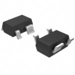 ATF-54143-TR1
The activity of extra discounts on wholesale prices is in full swing…
Please fill in your contact information and we will send you the latest wholesale price list.



