ChipApex | Global Electronic Components Supplier
SEARCH
Search Product
Search Post
— IC芯片 | 连接器 | 传感器 | 被动器件 —
Search productSearch post
— IC芯片 | 连接器 | 传感器 | 被动器件 —
Consult the customer manager about the wholesale price.
consultation hotline:86-132-6715-2157
email:[email protected]
Contact the product manager for consultation. One-stop consultation is available.
Do you want a lower wholesale price? Please send us your inquiry and we will reply immediately.
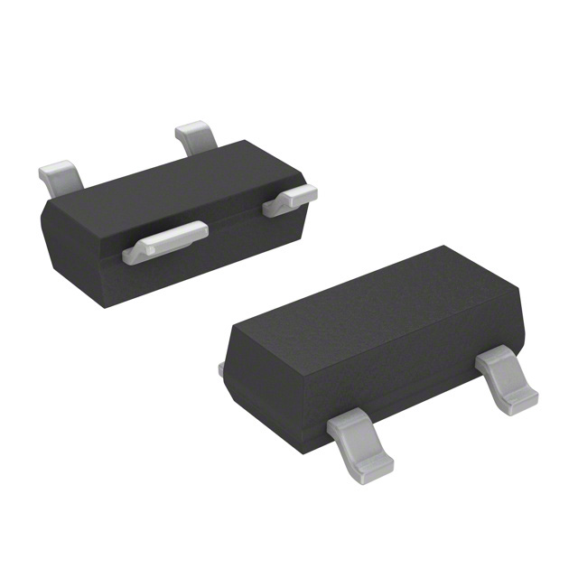
The BF1009SRE6327HTSA1 is a silicon N-channel MOSFET tetrode designed for low noise and high gain applications in controlled input stages up to 1 GHz. It features an integrated biasing network and operates at a voltage of 9 V. The device is housed in a surface-mount SOT-143R package with four pins, including Gate 1, Gate 2, Source, and Drain connections. Key electrical characteristics include a drain-source breakdown voltage of 12 V, a continuous drain current of 25 mA, and a total power dissipation of 200 mW. At 800 MHz, it provides a typical power gain of 22 dB and a noise figure of 1.4 dB.
Verify the specific suffix RE6327HTSA1 against official Infineon documentation to confirm packaging details and RoHS compliance status. Ensure that the ordering information matches the required SOT-143R variant. Confirm availability through authorized distributors as stock levels fluctuate. Cross-reference the datasheet revision date to ensure the latest technical specifications are applied during procurement.
Select this component when designing RF circuits requiring a low-noise, high-gain N-channel MOSFET tetrode. The integrated biasing network reduces external component count. Verify that the operating frequency remains within the 1 GHz limit and that the 9 V supply voltage aligns with system requirements. Consider the thermal resistance and power dissipation limits for proper heat management in the final assembly.
This part belongs to the BF1009S series of silicon N-channel MOSFET tetrodes manufactured by Infineon Technologies. The series is engineered for RF applications where low noise and high gain are critical. The BF1009SRE6327HTSA1 specifically denotes the SOT-143R package variant with tape-and-reel packaging. It shares core electrical characteristics with other BF1009S variants but differs in physical packaging and handling specifications.
No direct public substitutes are listed in the provided documentation. When evaluating alternatives, compare key parameters such as drain-source voltage, continuous drain current, power gain, and noise figure. Ensure the replacement device supports similar RF frequencies and has compatible pin configurations or requires schematic adjustments.
The device is designed for controlled input stages up to 1 GHz.
No, it features an integrated biasing network to simplify circuit design.
The typical power gain is 22 dB at 800 MHz with VDS = 9 V and VG2S = 6 V.


 BF1009SRE6327HTSA1
The activity of extra discounts on wholesale prices is in full swing…
Please fill in your contact information and we will send you the latest wholesale price list.