ChipApex | Global Electronic Components Supplier
SEARCH
Search Product
Search Post
— IC芯片 | 连接器 | 传感器 | 被动器件 —
Search productSearch post
— IC芯片 | 连接器 | 传感器 | 被动器件 —
Consult the customer manager about the wholesale price.
consultation hotline:86-132-6715-2157
email:[email protected]
Contact the product manager for consultation. One-stop consultation is available.
Do you want a lower wholesale price? Please send us your inquiry and we will reply immediately.
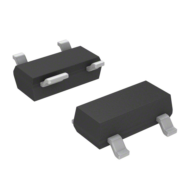
The BF1108R,235 is a silicon RF switch combining a depletion-type FET and a band-switching diode in an SOT143R package. It provides low insertion loss of up to 2 dB and high off-state isolation of at least 30 dB up to 1 GHz. Key electrical parameters include a drain-source on-state resistance of 12 Ω typical, gate-source pinch-off voltage of -4 V typical, and input/output capacitance of 0.65 pF typical. The device features integrated protection diodes between gate-source and gate-drain terminals.
Verify the specific ordering suffix matches the required package variant. Confirm that the component status aligns with current production requirements. Ensure handling procedures account for ElectroStatic Discharge sensitivity during transport and assembly. Cross-reference the marking code NHp to validate the physical unit received against the ordered specification.
Select this component when designing circuits requiring low-loss RF switching up to 1 GHz. The SOT143R package suits surface-mount layouts with reverse pinning configurations. Consider the integrated diode structure for simplified biasing networks. Evaluate the static and dynamic characteristics against system impedance requirements to ensure optimal signal integrity.
This part belongs to NXP's silicon RF switch portfolio, designed for general-purpose radio frequency applications. It utilizes a combination of field-effect transistor technology and band-switching diodes to achieve efficient signal routing. The product line supports various consumer electronics and communication equipment designs requiring reliable RF path control.
BF1108 serves as a direct functional equivalent utilizing the SOT143B package with standard pinning. Verify pin compatibility if substituting into existing PCB footprints designed for the reverse-pinning SOT143R variant.
The integrated diode isolates the MOSFET gate from ground, which contributes to achieving lower signal losses during operation.
Integrated diodes are placed between the gate-source and gate-drain terminals to protect the device against excessive input voltage surges.
Yes, the pinning information confirms that the drain and source connections are interchangeable for this device.
 BF1108R,235
The activity of extra discounts on wholesale prices is in full swing…
Please fill in your contact information and we will send you the latest wholesale price list.