 ChipApex | Global Electronic Components Supplier
SEARCH
Search Product
Search Post
— IC芯片 | 连接器 | 传感器 | 被动器件 —
Search productSearch post
— IC芯片 | 连接器 | 传感器 | 被动器件 —
Consult the customer manager about the wholesale price.
consultation hotline:86-132-6715-2157
email:[email protected]
Contact the product manager for consultation. One-stop consultation is available.
Do you want a lower wholesale price? Please send us your inquiry and we will reply immediately.
The BF1109WR,115 is an N-channel dual-gate enhancement-mode MOSFET in a SOT343R surface-mount package. It features a drain-source voltage of 11 V and a continuous drain current of 30 mA with total power dissipation of 200 mW at 80 °C. The device provides a forward transfer admittance of up to 30 mS and operates up to 1 GHz. Key dynamic parameters include a noise figure of 1.5 dB at 800 MHz and gate threshold voltages between 0.3 V and 1.2 V.
Verify the specific suffix WR corresponds to the SOT343R package variant during procurement. Confirm the product status as production data before initiating designs. Ensure anti-static handling protocols are followed due to ESD sensitivity. Cross-reference the latest datasheet revision to confirm pinning and thermal characteristics match the intended PCB layout requirements.
Select this component for RF applications requiring high forward transfer admittance relative to input capacitance. The dual-gate structure supports automatic gain control (AGC) functions effectively. Verify that the 11 V drain-source voltage rating aligns with the system supply voltage. Consider the SOT343R footprint constraints when designing the printed-circuit board layout.
This part belongs to the BF1109 series of N-channel dual-gate MOS-FETs manufactured by NXP Semiconductors. The BF1109WR specifically utilizes the SOT343R plastic surface-mounted package. It is designed for short-channel transistor applications where high frequency performance and low noise are critical requirements.
BF1109 and BF1109R are related variants within the same family but utilize different packages (SOT143B and SOT143R respectively). Verify pinout compatibility and physical dimensions before substituting these parts.
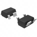 BF1109WR,115
The activity of extra discounts on wholesale prices is in full swing…
Please fill in your contact information and we will send you the latest wholesale price list.





