 ChipApex | Global Electronic Components Supplier
SEARCH
Search Product
Search Post
— IC芯片 | 连接器 | 传感器 | 被动器件 —
Search productSearch post
— IC芯片 | 连接器 | 传感器 | 被动器件 —
Consult the customer manager about the wholesale price.
consultation hotline:86-132-6715-2157
email:[email protected]
Contact the product manager for consultation. One-stop consultation is available.
Do you want a lower wholesale price? Please send us your inquiry and we will reply immediately.
The BF1204,135 is a dual N-channel dual gate MOS-FET discrete semiconductor component manufactured by NXP USA Inc. It integrates two equal amplifiers with shared source and gate leads within a SOT363 micro-miniature plastic package. The device features internal bias circuits for DC stabilization and integrated protection diodes between gates and the source to handle input voltage surges. Key electrical parameters include a drain-source voltage rating of 10 V, a maximum drain current of 30 mA, and a total power dissipation of 200 mW at temperatures up to 102 °C. Forward transfer admittance ranges from 25 mS to 40 mS at 1 MHz, while noise figures are specified as low as 0.9 dB at 400 MHz.
Verify the specific ordering suffix matches the required variant. Confirm that the component status aligns with current production requirements. Ensure compatibility with the target operating temperature range and supply voltage specifications. Review the most recently issued datasheet for any updates to pin configurations or absolute maximum ratings before finalizing design integration.
Select this component for designs requiring dual independent amplification channels with minimal footprint. The shared source architecture simplifies circuit layout compared to separate devices. Evaluate thermal resistance characteristics against expected power dissipation levels. Consider the specific noise figure requirements at target frequencies when determining suitability for sensitive RF front-end stages.
This component belongs to the NXP discrete semiconductors portfolio, specifically categorized under dual gate MOS-FETs. It is designed for high-frequency analog signal processing tasks where low noise and stable gain control are critical. The device utilizes a surface-mount package suitable for automated assembly processes in consumer electronics and professional communication hardware manufacturing lines.
Consult official NXP documentation for verified substitute part numbers. Cross-reference pinout configurations and electrical parameters carefully. Verify package dimensions match existing board layouts. Ensure functional equivalents meet all absolute maximum rating constraints.
Integrated diodes between the gates and source protect the device against excessive input voltage surges.
Internal bias circuits enable DC stabilization and provide very good cross-modulation performance during AGC operation.
The maximum drain-source voltage (VDS) rating is 10 V.


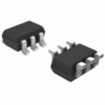 BF1204,135
The activity of extra discounts on wholesale prices is in full swing…
Please fill in your contact information and we will send you the latest wholesale price list.




