ChipApex | Global Electronic Components Supplier
SEARCH
Search Product
Search Post
— IC芯片 | 连接器 | 传感器 | 被动器件 —
Search productSearch post
— IC芯片 | 连接器 | 传感器 | 被动器件 —
Consult the customer manager about the wholesale price.
consultation hotline:86-132-6715-2157
email:[email protected]
Contact the product manager for consultation. One-stop consultation is available.
Do you want a lower wholesale price? Please send us your inquiry and we will reply immediately.
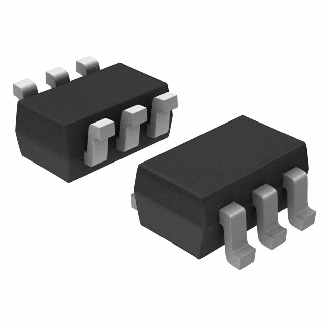
The BF1205C,115 is a dual N-channel dual gate MOS-FET in a SOT363 package. It integrates two amplifiers with shared source and gate leads plus an internal switch controlled by amplifier B's bias. Key electrical parameters include a drain-source voltage of 6 V, DC drain current of 30 mA, and total power dissipation of 180 mW. Forward transfer admittance ranges from 26 to 43 mS depending on the amplifier section. Input capacitance at Gate 1 is approximately 2.0 to 2.7 pF, while reverse transfer capacitance is 20 fF. Noise figures are 1.3 to 1.9 dB at 400 MHz and 1.4 to 2.1 dB at 800 MHz.
Verify the specific ordering suffix
Select this component when designing VHF/UHF low noise amplifiers requiring a 5 V supply. The device offers two distinct amplifier sections: one with fully integrated bias and another with partial integration. Ensure the design accommodates the 6 V maximum drain-source voltage and utilizes the internal switch functionality to minimize external circuitry complexity.
This part belongs to NXP Semiconductors' discrete RF MOSFET portfolio. It is designed as a specialized solution for tuners and communication systems where space constraints and signal integrity are critical. The dual-gate architecture allows for precise gain control and isolation between stages within a micro-miniature plastic package.
No public confirmed substitute part numbers are available in the documentation.
The integrated switch is operated by the gate 1 bias of amplifier b.
Integrated diodes between the gates and source protect the device against excessive input voltage surges.
Yes, the device features internal bias circuits that enable DC stabilization and superior cross-modulation performance specifically during AGC operation.
 BF1205C,115
The activity of extra discounts on wholesale prices is in full swing…
Please fill in your contact information and we will send you the latest wholesale price list.