ChipApex | Global Electronic Components Supplier
SEARCH
Search Product
Search Post
— IC芯片 | 连接器 | 传感器 | 被动器件 —
Search productSearch post
— IC芯片 | 连接器 | 传感器 | 被动器件 —
Consult the customer manager about the wholesale price.
consultation hotline:86-132-6715-2157
email:[email protected]
Contact the product manager for consultation. One-stop consultation is available.
Do you want a lower wholesale price? Please send us your inquiry and we will reply immediately.
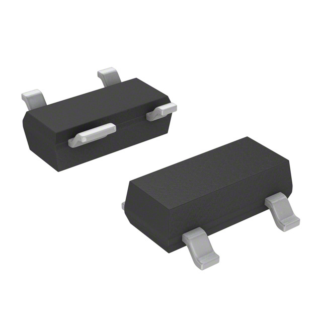
The BF1211R,215 is an N-channel dual-gate MOS-FET in the SOT143R package. It features a drain-source voltage of 6 V and a continuous drain current of 30 mA with total power dissipation of 180 mW. The forward transfer admittance ranges from 25 to 40 mS, while input capacitance at gate 1 is typically 2.1 pF. Noise figures are 0.9 dB at 400 MHz and 3.5 dB at 11 MHz. Junction temperature reaches 150 °C.
Verify the specific ordering suffix
Select this component when designing low noise amplifiers requiring dual-gate isolation for improved stability and reduced feedback. The SOT143R package suits surface mount designs needing reverse pinning compatibility. Ensure operating conditions remain within the 6 V drain-source limit and 180 mW power dissipation threshold to maintain reliability.
This device belongs to the BF1211 series of N-channel dual-gate MOS-FETs manufactured by NXP Semiconductors. It shares core electrical characteristics with the BF1211 and BF1211WR variants but utilizes the SOT143R plastic surface-mounted package with reverse pinning configuration for distinct board layout requirements.
Direct replacements include the BF1211 (SOT143B) and BF1211WR (SOT343R). Verify pinout orientation differences due to reverse pinning variations before substitution.
The dual-gate structure allows independent control of gain via Gate 2 while maintaining signal input at Gate 1, providing better isolation and reduced feedback compared to single-gate devices.
The maximum junction temperature (Tj) is rated at 150 °C.


 BF1211R,215
The activity of extra discounts on wholesale prices is in full swing…
Please fill in your contact information and we will send you the latest wholesale price list.