ChipApex | Global Electronic Components Supplier
SEARCH
Search Product
Search Post
— IC芯片 | 连接器 | 传感器 | 被动器件 —
Search productSearch post
— IC芯片 | 连接器 | 传感器 | 被动器件 —
Consult the customer manager about the wholesale price.
consultation hotline:86-132-6715-2157
email:[email protected]
Contact the product manager for consultation. One-stop consultation is available.
Do you want a lower wholesale price? Please send us your inquiry and we will reply immediately.
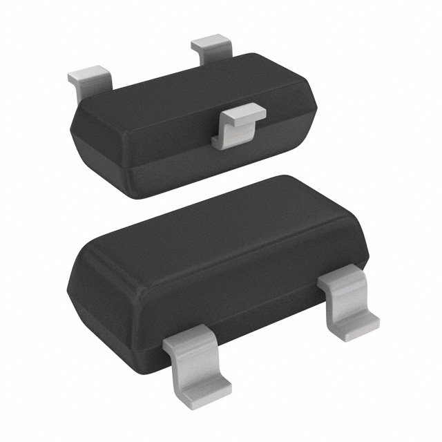
The BF545C,215 is an N-channel symmetrical silicon junction field-effect transistor housed in a SOT23 plastic surface-mounted package. It features a drain-source voltage rating of ±30 V and a total power dissipation of 250 mW at 25 °C ambient temperature. The device exhibits a gate-source cut-off voltage range of -3.2 V to -7.8 V and a drain current capability between 12 mA and 25 mA under standard test conditions. Forward transfer admittance is specified from 3 mS to 6.5 mS.
Verify the specific ordering suffix matches the required manufacturing origin code (P, T, or W) as indicated by the marking table. Confirm that the component status aligns with current production availability through official NXP channels before finalizing design-in decisions.
Select this variant when a higher gate-source cut-off voltage and drain current are required compared to the BF545A or BF545B models. Ensure the application operates within the absolute maximum ratings, particularly regarding thermal resistance and junction temperature limits during high-frequency operation.
This component belongs to the BF545 family of N-channel silicon JFETs manufactured by NXP Semiconductors. The family includes variants A, B, and C, differentiated primarily by their gate-source cut-off voltage and drain current specifications while sharing the same SOT23 package and general electrical characteristics.
BF545A,215; BF545B,215
Pin 1 is the source, Pin 2 is the drain, and Pin 3 is the gate.
The BF545C has a higher gate-source cut-off voltage range (-3.2 V to -7.8 V) and higher drain current (12 mA to 25 mA) compared to the BF545A (-0.4 V to -2.2 V and 2 mA to 6.5 mA).
No, unless expressly stated in the data sheet, this product is not suitable for automotive use and is not qualified according to automotive testing requirements.



 BF545C,215
The activity of extra discounts on wholesale prices is in full swing…
Please fill in your contact information and we will send you the latest wholesale price list.