ChipApex | Global Electronic Components Supplier
SEARCH
Search Product
Search Post
— IC芯片 | 连接器 | 传感器 | 被动器件 —
Search productSearch post
— IC芯片 | 连接器 | 传感器 | 被动器件 —
Consult the customer manager about the wholesale price.
consultation hotline:86-132-6715-2157
email:[email protected]
Contact the product manager for consultation. One-stop consultation is available.
Do you want a lower wholesale price? Please send us your inquiry and we will reply immediately.
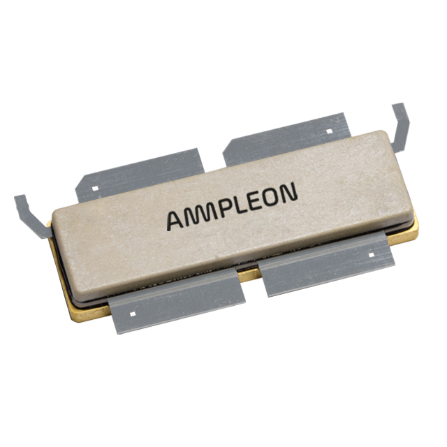
The BLC10G22XS-551AVTZ is a 550 W LDMOS asymmetric Doherty power transistor designed for base station applications in the 2100 MHz to 2200 MHz frequency range. It features a drain-source breakdown voltage of 65 V and operates with a case temperature range from -40 °C to +125 °C. In an asymmetrical Doherty test circuit at 32 V, it delivers typical average output powers of 90 W to 115 W with drain efficiencies between 49.8% and 50.5%. The device exhibits a power gain of approximately 15.9 dB to 16.3 dB and an adjacent channel power ratio (ACPR) of -28.5 dBc to -29.1 dBc under 1-carrier W-CDMA conditions.
Verify the specific ordering suffix against official Ampleon documentation to confirm packaging variations. Confirm RoHS compliance status directly through manufacturer channels. Ensure handling procedures meet ESD sensitivity requirements specified in the datasheet. Validate thermal management solutions align with junction-to-case resistance limits. Cross-reference part numbers with authorized distributors to ensure authenticity.
Evaluate the device's suitability for asymmetric Doherty topologies requiring high efficiency and linearity. Consider the internal matching network when designing input and output impedance circuits. Assess thermal dissipation capabilities based on the specified junction-to-case resistance values. Verify that the operating frequency range matches the target application spectrum. Review load-pull data to determine optimal source and load impedances for peak performance.
This component belongs to the BLC10G22XS series of LDMOS transistors manufactured by Ampleon. These devices are engineered for high-power RF applications, specifically targeting the evolution of wireless communication infrastructure. The series utilizes advanced LDMOS technology to deliver robust performance in demanding base station environments.
Consult official Ampleon substitution guides for verified equivalent parts. Do not assume functional compatibility with other LDMOS families without rigorous testing. Verify pinout and package dimensions match existing board layouts. Check if alternative parts offer comparable ruggedness and thermal characteristics.
The BLC10G22XS-551AVT can withstand a load mismatch corresponding to a VSWR of 10:1 through all phases under specified operating conditions.
For the main device, the typical gate-source quiescent voltage is 2.2 V when measured at a drain-source voltage of 32 V and a drain current of 800 mA.
The device holds a Charged Device Model (CDM) classification of C3 and a Human Body Model (HBM) classification of 2.



 BLC10G22XS-551AVTZ
The activity of extra discounts on wholesale prices is in full swing…
Please fill in your contact information and we will send you the latest wholesale price list.