ChipApex | Global Electronic Components Supplier
SEARCH
Search Product
Search Post
— IC芯片 | 连接器 | 传感器 | 被动器件 —
Search productSearch post
— IC芯片 | 连接器 | 传感器 | 被动器件 —
Consult the customer manager about the wholesale price.
consultation hotline:86-132-6715-2157
email:[email protected]
Contact the product manager for consultation. One-stop consultation is available.
Do you want a lower wholesale price? Please send us your inquiry and we will reply immediately.
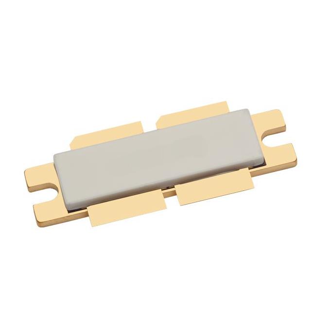
The BLF178P,112 is a dual N-channel LDMOS power transistor designed for broadcast and industrial applications in the HF to 110 MHz band. It operates with a drain-source voltage of 50 V and delivers up to 1200 W output power at 108 MHz under pulsed conditions (tp=100 µs, duty cycle 20%). The device achieves a typical power gain of 28.5 dB and drain efficiency of 75%. Key DC parameters include a breakdown voltage of 110 V, threshold voltage of 1.7 V, and maximum drain current of 88 A. Thermal resistance from junction to case is 0.14 K/W. It utilizes a flanged balanced ceramic SOT539A package.
Verify component authenticity through official Ampleon channels or authorized distributors. Confirm that the ordering suffix matches the required packaging specifications. Ensure compliance with RoHS directives as stated in the product data sheet. Validate supply chain integrity to prevent counterfeit components. Review the latest datasheet revision for any updates to electrical characteristics or handling instructions before procurement.
Select this component for applications requiring high power density in the HF to VHF bands. Ensure the design accommodates the 50 V drain supply and manages the 0.14 K/W thermal resistance effectively. Verify that the load impedance matches the simulated values for optimal performance. Consider the pulsed operation limits when designing for peak power scenarios. Evaluate the need for ESD protection measures during handling and assembly.
The BLF178P belongs to Ampleon's portfolio of LDMOS power transistors engineered for robust RF performance. It represents a transition from previous Philips/NXP generations, maintaining compatibility with established designs while offering enhanced reliability. The device is part of a family optimized for broadcast infrastructure, providing a balance between high output power and efficient energy conversion in wideband applications.
Check for updated revisions within the BLF178P series. Consult Ampleon documentation for direct pin-compatible alternatives if specific package variants are unavailable. Verify that any substitute maintains the same thermal and electrical ratings for the target application.
The device can withstand a load mismatch corresponding to a Voltage Standing-Wave Ratio (VSWR) of 13:1 through all phases under specified operating conditions.
The gate-source quiescent voltage (VGSq) is typically 1.3 V when measured with a drain-source voltage of 50 V and a quiescent drain current of 20 mA.
The transient thermal impedance from junction to case (Zth(j-c)) is 0.04 K/W for a pulse duration of 100 µs with a 20% duty cycle at a junction temperature of 150 °C.
 BLF178P,112
The activity of extra discounts on wholesale prices is in full swing…
Please fill in your contact information and we will send you the latest wholesale price list.