ChipApex | Global Electronic Components Supplier
SEARCH
Search Product
Search Post
— IC芯片 | 连接器 | 传感器 | 被动器件 —
Search productSearch post
— IC芯片 | 连接器 | 传感器 | 被动器件 —
Consult the customer manager about the wholesale price.
consultation hotline:86-132-6715-2157
email:[email protected]
Contact the product manager for consultation. One-stop consultation is available.
Do you want a lower wholesale price? Please send us your inquiry and we will reply immediately.
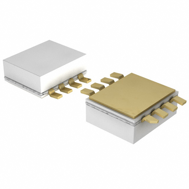
The BLF404,115 is a silicon N-channel enhancement mode vertical D-MOS power transistor manufactured by Ampleon USA Inc. It is housed in an 8-lead SOT409A surface-mount package with a ceramic cap. Designed for broadband operation, the device operates at a nominal supply voltage of 12.5 V and delivers a continuous wave output power of 4 W at 500 MHz. Key electrical parameters include a drain-source breakdown voltage of 40 V, a maximum total power dissipation of 8.3 W at a mounting base temperature of 85 °C, and a thermal resistance from junction to mounting base of 12.1 K/W.
Verify the specific ordering suffix against official Ampleon documentation to confirm exact packaging or binning specifications. Ensure that any referenced datasheet corresponds to the current production status. Confirm compatibility with standard SMD reflow soldering profiles for the SOT409A package before initiating procurement processes.
Select this component for applications requiring a 12.5 V supply and approximately 4 W output power at 500 MHz. The device is optimized for Class-AB operation with a minimum power gain of 10 dB. Designers must account for the 12.1 K/W thermal resistance and ensure the mounting base temperature remains within specified limits to maintain reliable operation.
This component is part of the UHF power MOS transistor family originally developed by Philips Semiconductors. Following corporate restructuring, the product line was transferred to Ampleon, which now manages the specification and distribution. The BLF404 represents a legacy design adapted for modern surface-mount manufacturing processes while maintaining the electrical characteristics of its predecessors.
Consult official substitution lists for compatible devices such as the BLF521, BLF522, BLF542, BLF543, or BLF544. Verify pinout compatibility and thermal requirements before replacing the original component in existing designs.
The absolute maximum drain-source voltage (VDS) is rated at 40 V.
The BLF404 is designed to withstand full load mismatch conditions corresponding to a VSWR of 10:1 through all phases during Class-AB operation.
It is recommended to mount the transistor on a grounded metallized area of the PCB with at least 12 x 0.5 mm diameter through metallized holes filled with solder to achieve a thermal resistance of 5 K/W from the mounting base to the heatsink.



 BLF404,115
The activity of extra discounts on wholesale prices is in full swing…
Please fill in your contact information and we will send you the latest wholesale price list.