ChipApex | Global Electronic Components Supplier
SEARCH
Search Product
Search Post
— IC芯片 | 连接器 | 传感器 | 被动器件 —
Search productSearch post
— IC芯片 | 连接器 | 传感器 | 被动器件 —
Consult the customer manager about the wholesale price.
consultation hotline:86-132-6715-2157
email:[email protected]
Contact the product manager for consultation. One-stop consultation is available.
Do you want a lower wholesale price? Please send us your inquiry and we will reply immediately.
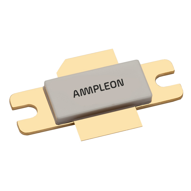
The BLF6G10-200RN is a 200 W LDMOS power transistor designed for base station applications in the 700 MHz to 1000 MHz frequency range. It operates with a drain-source voltage of 28 V and features an internal matching network for simplified integration. The device exhibits high efficiency, excellent thermal stability, and enhanced ruggedness capable of withstanding a VSWR of 10:1. Typical performance at 869 MHz to 894 MHz includes a 40 W average output power, 20 dB power gain, 28.5% drain efficiency, and -39 dBc ACPR under 2-carrier W-CDMA conditions.
Verify the specific package variant required for the design. The BLF6G10-200RN utilizes the SOT502A flanged ceramic package with mounting holes, whereas the BLF6G10LS-200RN uses the SOT502B earless flanged package. Confirm that the ordering suffix matches the physical footprint requirements before finalizing procurement orders.
Select this component for high-power RF amplifier designs operating between 700 MHz and 1000 MHz. Ensure the application circuit can maintain the case temperature within specified limits, as thermal resistance varies between the SOT502A and SOT502B packages. Verify that the gate biasing network supports the quiescent current requirements for the intended modulation scheme.
This part belongs to Ampleon's LDMOS power transistor portfolio, specifically engineered for cellular infrastructure. It serves as a successor to earlier NXP semiconductor designs in the same frequency band. The device is optimized for linear amplification in multi-standard base station environments requiring high linearity and power density.
The BLF6G10LS-200RN is a direct functional equivalent but utilizes the SOT502B earless package instead of the SOT502A flanged package. Substitution requires verification of mechanical mounting constraints and PCB layout compatibility due to the differing package outlines.
 BLF6G10-200RN,112
The activity of extra discounts on wholesale prices is in full swing…
Please fill in your contact information and we will send you the latest wholesale price list.