ChipApex | Global Electronic Components Supplier
SEARCH
Search Product
Search Post
— IC芯片 | 连接器 | 传感器 | 被动器件 —
Search productSearch post
— IC芯片 | 连接器 | 传感器 | 被动器件 —
Consult the customer manager about the wholesale price.
consultation hotline:86-132-6715-2157
email:[email protected]
Contact the product manager for consultation. One-stop consultation is available.
Do you want a lower wholesale price? Please send us your inquiry and we will reply immediately.
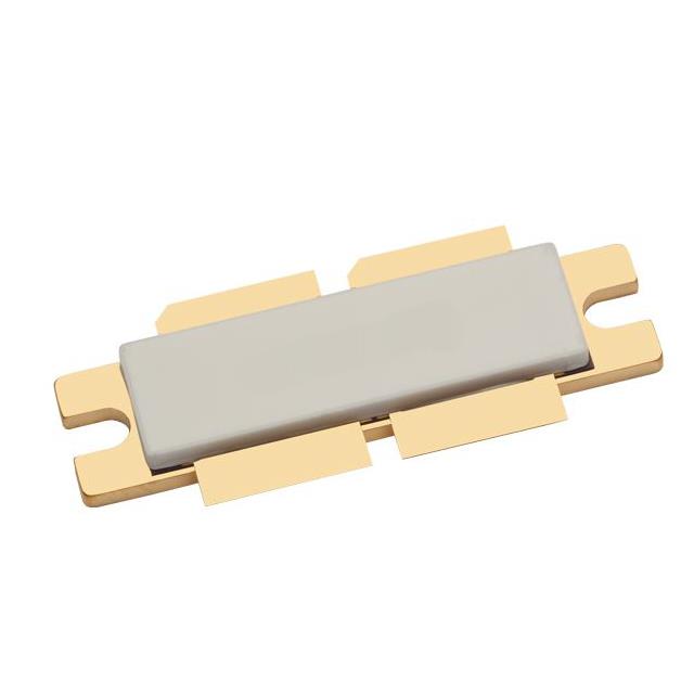
The BLF6G20-230PRN is a 230 W LDMOS power transistor designed for base station applications operating between 1800 MHz and 2000 MHz. It features an internally matched balanced ceramic package (SOT539A) with two mounting holes and four leads. The device operates at a supply voltage of 28 V, delivering typical average output powers of 65 W in dual-carrier W-CDMA mode and up to 125 W in single-carrier configurations. Key electrical parameters include a drain-source breakdown voltage of 65 V, a junction temperature limit of 225 °C, and a thermal resistance from junction to case of 0.38 K/W.
Verify component authenticity by checking the manufacturer's official documentation against the specific part number. Ensure that the ordering suffix matches the required package variant, as physical differences exist between flanged and earless versions. Confirm RoHS compliance status based on the latest product specifications provided by the manufacturer before finalizing procurement orders.
Select this component for broadband RF power amplifier designs requiring high efficiency and ruggedness within the 1800 MHz to 2000 MHz spectrum. Consider the SOT539A package dimensions and mounting hole requirements during PCB layout. Evaluate thermal management strategies to maintain case temperatures within specified limits under maximum power load conditions.
This device belongs to Ampleon's portfolio of LDMOS power transistors engineered for telecommunications infrastructure. It serves as a critical active element in radio frequency power amplification stages, specifically optimized for wideband code division multiple access systems. The component represents a balance of high power density and operational reliability for modern cellular network deployments.
The BLF6G20S-230PRN is a verified substitute featuring an earless flanged balanced ceramic package (SOT539B). Verify mechanical compatibility regarding mounting hole placement and lead configuration when substituting between these variants.
The maximum junction temperature is rated at 225 °C.
It can withstand a load mismatch corresponding to a VSWR of 10:1 through all phases under specified operating conditions.
The typical drain efficiency is 32% at an average output power of 65 W in dual-carrier W-CDMA operation.


 BLF6G20-230PRN,118
The activity of extra discounts on wholesale prices is in full swing…
Please fill in your contact information and we will send you the latest wholesale price list.