ChipApex | Global Electronic Components Supplier
SEARCH
Search Product
Search Post
— IC芯片 | 连接器 | 传感器 | 被动器件 —
Search productSearch post
— IC芯片 | 连接器 | 传感器 | 被动器件 —
Consult the customer manager about the wholesale price.
consultation hotline:86-132-6715-2157
email:[email protected]
Contact the product manager for consultation. One-stop consultation is available.
Do you want a lower wholesale price? Please send us your inquiry and we will reply immediately.
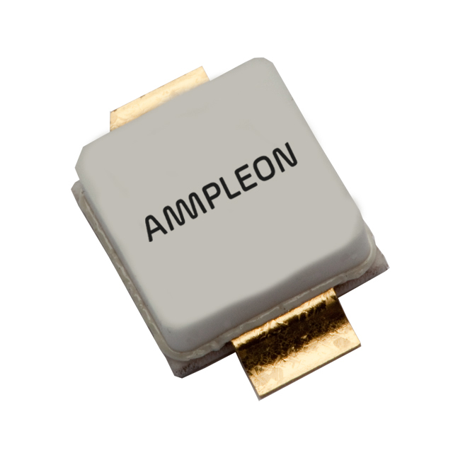
The BLF6G27-10G,118 is a dual N-channel LDMOS RF power transistor manufactured by Ampleon USA Inc. Designed for broadband applications in the 2300 MHz to 2700 MHz frequency range, this component utilizes advanced silicon LDMOS technology. It features a robust construction suitable for high-power density operations, typically delivering significant output power with high gain efficiency. The device is housed in a surface-mount SOT511 package, facilitating integration into compact RF amplifier modules and base station architectures requiring reliable performance across wide bandwidths.
Verify the specific suffix '118' against the official Ampleon datasheet to confirm tape-and-reel packaging specifications. Confirm RoHS compliance status and check for any Product Change Notifications (PCN) related to manufacturing site transfers or material updates. Ensure compatibility with existing PCB footprints for the SOT511 package before finalizing procurement orders.
Select this component when designing amplifiers for the 2300-2700 MHz band requiring dual-channel symmetry. Evaluate thermal management requirements based on the specified drain voltage and output power levels. Compare gain and linearity metrics against alternative LDMOS devices in the same family to ensure optimal system efficiency and impedance matching network design.
This part belongs to the BLF6G series of broadband LDMOS transistors from Ampleon. The series is engineered for cost-effective, high-volume production of RF power amplifiers. The '27' designation typically indicates the target frequency band around 2.7 GHz, while '10G' often refers to specific gain or power variants within the product line. These devices are foundational components in modern mobile telecommunications infrastructure.
Consult the Ampleon replacement guide for direct equivalents within the BLF6G family. Verify pinout compatibility and thermal characteristics if substituting with other SOT511 packages. Cross-reference electrical parameters such as Vds, Pd, and Gain to ensure the alternative meets the original circuit design constraints without requiring significant schematic modifications.
 BLF6G27-10G,118
The activity of extra discounts on wholesale prices is in full swing…
Please fill in your contact information and we will send you the latest wholesale price list.