ChipApex | Global Electronic Components Supplier
SEARCH
Search Product
Search Post
— IC芯片 | 连接器 | 传感器 | 被动器件 —
Search productSearch post
— IC芯片 | 连接器 | 传感器 | 被动器件 —
Consult the customer manager about the wholesale price.
consultation hotline:86-132-6715-2157
email:[email protected]
Contact the product manager for consultation. One-stop consultation is available.
Do you want a lower wholesale price? Please send us your inquiry and we will reply immediately.
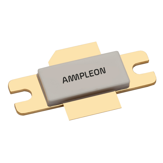
The BLF6G38-100 is a 100 W LDMOS power transistor designed for base station applications in the 3400 MHz to 3600 MHz frequency range. It operates at a supply voltage of 28 V with a drain-source breakdown voltage of 65 V and a maximum gate-source voltage of 13 V. The device delivers an average output power of 18.5 W and a peak output power of 130 W, achieving a typical power gain of 13 dB and a drain efficiency of 21.5%. It features integrated ESD protection, excellent ruggedness capable of withstanding a VSWR of 10:1, and low thermal resistance ranging from 0.43 K/W to 0.58 K/W depending on the package variant.
Verify the specific package variant required for the design, as the BLF6G38-100 corresponds to the SOT502A flanged ceramic package with mounting holes, while the BLF6G38LS-100 uses the SOT502B earless flanged package. Confirm that the ordering suffix matches the intended mechanical footprint before procurement. Ensure all handling procedures account for the device's sensitivity to electrostatic discharge during transport and assembly.
Select this component for wideband RF power amplifier designs operating between 3400 MHz and 3600 MHz. The device supports single-carrier N-CDMA and WiMAX signals with high linearity and efficiency. Consider the thermal resistance specifications when designing heat sinks, noting the difference between the SOT502A and SOT502B packages. Ensure the application circuit can handle the peak output power of 130 W and the specified load mismatch conditions.
This part belongs to Ampleon's LDMOS power transistor portfolio targeting wireless infrastructure. It is specifically engineered for the 3.4 GHz to 3.6 GHz spectrum, commonly used for WiMAX and other broadband wireless access technologies. The product line emphasizes ruggedness and efficiency for demanding base station environments.
The BLF6G38LS-100 serves as a mechanical alternative within the same electrical family, utilizing the SOT502B earless flanged package instead of the SOT502A. Verify that the PCB layout accommodates the specific lead configuration of the chosen variant. No other direct cross-model substitutes are documented in the official data sheet.


 BLF6G38-100,112
The activity of extra discounts on wholesale prices is in full swing…
Please fill in your contact information and we will send you the latest wholesale price list.