ChipApex | Global Electronic Components Supplier
SEARCH
Search Product
Search Post
— IC芯片 | 连接器 | 传感器 | 被动器件 —
Search productSearch post
— IC芯片 | 连接器 | 传感器 | 被动器件 —
Consult the customer manager about the wholesale price.
consultation hotline:86-132-6715-2157
email:[email protected]
Contact the product manager for consultation. One-stop consultation is available.
Do you want a lower wholesale price? Please send us your inquiry and we will reply immediately.
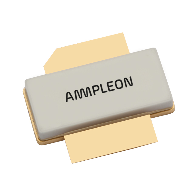
The BLF7G10LS-250 is a 250 W LDMOS power transistor designed for base station applications in the 869 MHz to 960 MHz frequency range. It operates with a drain-source voltage of 30 V and quiescent current of 1800 mA, delivering 60 W average output power. The device provides a typical power gain of 19.5 dB and drain efficiency up to 30.5% under two-carrier W-CDMA conditions. It features an earless flanged ceramic package (SOT502B) with integrated ESD protection and internal matching for input and output circuits.
Verify the specific ordering suffix against official Ampleon documentation to confirm package variations and compliance status. Ensure that procurement channels provide valid traceability for this RF power component. Confirm RoHS Directive 2002/95/EC compliance through manufacturer certificates prior to integration into production environments.
Select the BLF7G10LS-250 variant specifically when an earless flanged ceramic package (SOT502B) is required for the design. Verify thermal management capabilities against the junction-to-case thermal resistance of 0.38 K/W at Tcase = 80 °C. Ensure the application circuit supports the specified 30 V drain-source voltage and 1800 mA quiescent current requirements for optimal performance.
This component belongs to the BLF7G10L-250 family from Ampleon. The LS suffix denotes the SOT502B earless flanged ceramic package, distinguishing it from the standard SOT502A flanged package with mounting holes found in the BLF7G10L-250 variant. Both share identical electrical specifications and are intended for broadband RF power amplifier designs.
The BLF7G10L-250 serves as a direct functional substitute if the mechanical footprint allows for the SOT502A package with mounting holes. Verify PCB layout compatibility regarding lead positions and thermal dissipation paths before substituting between the SOT502A and SOT502B package variants.
The device can withstand a load mismatch corresponding to VSWR = 10:1 through all phases under CW conditions of 200 W at 920 MHz to 960 MHz.
No, unless expressly stated otherwise, this product is not automotive qualified and is not suitable for automotive equipment or applications.
The typical drain efficiency is 30.5% at 60 W average output power under two-carrier W-CDMA test conditions.
 BLF7G10LS-250,118
The activity of extra discounts on wholesale prices is in full swing…
Please fill in your contact information and we will send you the latest wholesale price list.