ChipApex | Global Electronic Components Supplier
SEARCH
Search Product
Search Post
— IC芯片 | 连接器 | 传感器 | 被动器件 —
Search productSearch post
— IC芯片 | 连接器 | 传感器 | 被动器件 —
Consult the customer manager about the wholesale price.
consultation hotline:86-132-6715-2157
email:[email protected]
Contact the product manager for consultation. One-stop consultation is available.
Do you want a lower wholesale price? Please send us your inquiry and we will reply immediately.
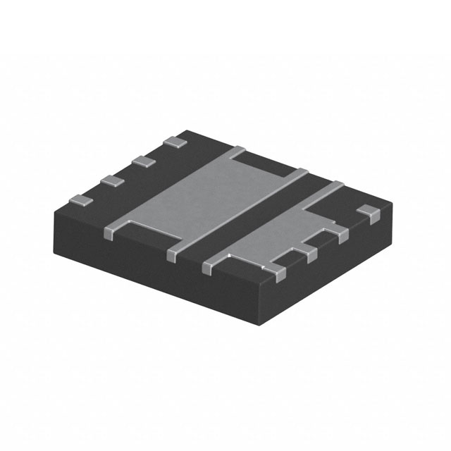
The BSC0923NDIATMA1 is a dual N-channel OptiMOS™ MOSFET designed for high-performance buck converters. It features logic-level operation rated at 4.5V and includes monolithic Schottky-like diodes. The device utilizes PG-TISON-8 packaging and is qualified according to JEDEC standards. Key electrical parameters include a drain-source breakdown voltage of 30V, continuous drain current up to 40A, and maximum on-state resistance of 7.0mΩ at VGS=10V. It operates within a temperature range of -55°C to +150°C.
Verify the component against official Infineon datasheets to confirm technical specifications and package integrity. Ensure compatibility with target circuit requirements regarding thermal management and voltage ratings. Confirm that the ordering suffix matches the required tape-and-reel configuration for automated assembly processes.
Select this component for designs requiring low gate charge and fast switching speeds in compact footprints. The logic-level threshold simplifies driver interface requirements. Evaluate thermal performance based on specific PCB copper area constraints, as power dissipation varies significantly between minimum footprint and standard cooling configurations.
This part belongs to the OptiMOS™ family of power MOSFETs from Infineon Technologies. It represents a dual-channel configuration integrating two N-channel devices into a single package. The technology focuses on minimizing conduction losses while maintaining robust switching characteristics suitable for modern power supply architectures.
Consult official Infineon documentation for verified substitute part numbers. Cross-reference pinouts and electrical limits before implementation.
Yes, the device is qualified according to JEDEC standards for target applications, which typically include automotive environments.
The maximum operating and storage temperature range extends up to +150°C.
Yes, it features monolithically integrated Schottky-like diodes for each channel.
 BSC0923NDIATMA1
The activity of extra discounts on wholesale prices is in full swing…
Please fill in your contact information and we will send you the latest wholesale price list.