 ChipApex | Global Electronic Components Supplier
SEARCH
Search Product
Search Post
— IC芯片 | 连接器 | 传感器 | 被动器件 —
Search productSearch post
— IC芯片 | 连接器 | 传感器 | 被动器件 —
Consult the customer manager about the wholesale price.
consultation hotline:86-132-6715-2157
email:[email protected]
Contact the product manager for consultation. One-stop consultation is available.
Do you want a lower wholesale price? Please send us your inquiry and we will reply immediately.
The BSL207NH6327XTSA1 is a dual N-channel enhancement-mode MOSFET from the OptiMOS™2 series, housed in a TSOP-6 surface-mount package. It features a drain-source voltage of 20 V and a continuous drain current of 2.1 A at 25 °C. The device has a maximum on-state resistance of 70 mΩ at VGS=4.5 V and 110 mΩ at VGS=2.5 V. Rated for avalanche energy operation, it supports a total power dissipation of 0.5 W and operates within a temperature range of -55 °C to 150 °C.
Verify the specific ordering suffix H6327 to confirm tape and reel packaging quantities. Ensure the component meets RoHS compliance and halogen-free requirements per IEC61249-2-21 standards before integration into final assemblies.
Select this component when a dual N-channel solution is required in a compact TSOP-6 footprint. The low gate threshold voltage makes it suitable for direct interfacing with low-voltage logic controllers. Verify thermal management capabilities as power dissipation is limited to 0.5 W.
This part belongs to Infineon's OptiMOS™2 family of small-signal transistors. These devices are designed for general-purpose switching applications where low on-resistance and fast switching speeds are prioritized. The dual configuration allows for space-efficient circuit designs compared to using discrete single-channel transistors.
BSL207N
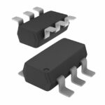 BSL207NH6327XTSA1
The activity of extra discounts on wholesale prices is in full swing…
Please fill in your contact information and we will send you the latest wholesale price list.





