ChipApex | Global Electronic Components Supplier
SEARCH
Search Product
Search Post
— IC芯片 | 连接器 | 传感器 | 被动器件 —
Search productSearch post
— IC芯片 | 连接器 | 传感器 | 被动器件 —
Consult the customer manager about the wholesale price.
consultation hotline:86-132-6715-2157
email:[email protected]
Contact the product manager for consultation. One-stop consultation is available.
Do you want a lower wholesale price? Please send us your inquiry and we will reply immediately.
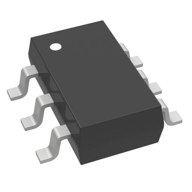
The BSL316CH6327XTSA1 is a small signal complementary MOSFET featuring an N-channel and P-channel enhancement mode in a PG-TSOP-6 package. It operates with a drain-source voltage of ±30 V, continuous drain currents of 1.4 A (N) and -1.5 A (P), and on-state resistances of 160 mΩ (N) and 150 mΩ (P). The device supports a power dissipation of 0.5 W at 25 °C, withstands avalanche energy up to 11 mJ, and functions within a temperature range of -55 °C to +150 °C.
Verify the specific ordering suffix H6327XTSA1 against official Infineon documentation to confirm tape and reel packaging specifications. Ensure compliance with RoHS and halogen-free requirements as stated in the datasheet. Confirm that the component meets AEC-Q101 qualification criteria if intended for automotive applications. Cross-reference the PG-TSOP-6 footprint dimensions during PCB layout validation.
Select this component when a complementary pair is required in a minimal footprint. The logic level rating supports direct interfacing with standard digital logic outputs. Consider the thermal resistance and power dissipation limits relative to the ambient temperature and duty cycle. Verify that the 30 V breakdown voltage aligns with the circuit's maximum operating voltage.
This part belongs to the BSL316C series of OptiMOS™ 2 and OptiMOS™-P 2 small signal transistors. It represents a complementary technology combining silicon N-channel and P-channel structures. The series is designed for applications demanding low on-resistance and high switching speed in a compact TSOP-6 package.
BSL316CH6327XTSA1
 BSL316CH6327XTSA1
The activity of extra discounts on wholesale prices is in full swing…
Please fill in your contact information and we will send you the latest wholesale price list.