 ChipApex | Global Electronic Components Supplier

SEARCH
Search Product
Search Post
— IC芯片 | 连接器 | 传感器 | 被动器件 —
Search productSearch post
— IC芯片 | 连接器 | 传感器 | 被动器件 —
Consult the customer manager about the wholesale price.
consultation hotline:86-132-6715-2157
email:[email protected]
Contact the product manager for consultation. One-stop consultation is available.
Do you want a lower wholesale price? Please send us your inquiry and we will reply immediately.
The BSS806NH6327XTSA1 is an N-channel enhancement mode MOSFET from the OptiMOS™ 2 series. It features a maximum drain-source voltage of 20 V and continuous drain current of 2.3 A at 25 °C. The device has a maximum on-state resistance of 57 mΩ at VGS=2.5 V and 82 mΩ at VGS=1.8 V. Total gate charge is 1.7 nC, with a threshold voltage range of 0.3 V to 0.75 V. Power dissipation is 0.5 W at 25 °C in a PG-SOT23 package.
Verify the complete part number including the H6327 suffix against official Infineon documentation to confirm packaging and tape-and-reel specifications. Ensure compatibility with surface mount assembly processes by checking soldering temperature limits and ESD handling requirements specified in the datasheet.
Select this component when low gate drive voltage is required, specifically for logic levels around 1.8 V or 2.5 V. The small-signal SOT-23 package suits space-constrained designs. Verify that the 20 V breakdown voltage and 2.3 A current rating align with the specific circuit load requirements.
This part belongs to the BSS806N family within Infineon's OptiMOS™ 2 portfolio. These are small-signal transistors designed for efficient switching in compact form factors. The technology focuses on minimizing gate charge and on-resistance for improved efficiency in low-voltage environments.
Check for direct substitutes within the BSS806N family or other OptiMOS™ 2 variants. Confirm pinout compatibility and electrical parameter equivalence before substitution.
The maximum gate-source voltage is ±8 V.
Yes, the BSS806N is avalanche rated with a single pulse energy of 10.8 mJ at ID=2.3 A.
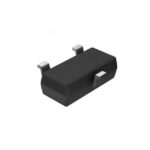 BSS806NH6327XTSA1

The activity of extra discounts on wholesale prices is in full swing…
Please fill in your contact information and we will send you the latest wholesale price list.





